
Homemade Printed Circuit Boards - Part1: Intro
This is the first part of a three-part series detailing the process of creating a double-sided printed circuit board at home with pretty good accuracy. With this comes the ability to create experimental modules and breakout boards of nearly any SMD part we salvage. Throughout the series, we shall look at toner transfer, PCB etching, creating through vias as well as SMD component assembly techniques all done by hand.
Motherboards are called so because they have separate daughter boards that are usually mounted on them to make up a complete system (e.g. a computer motherboard has RAM boards mounted on it). Both of these boards consist of individual electronic components connected as a circuit on the boards thus the general name for them is circuit boards. And since the process of creating circuit boards involves printing a circuit design onto said board using various techniques, you will often see them referred to as printed circuit boards.
What is a PCB and why use it?
A Printed circuit board (PCB) is a common board where all electrical components that make up a circuit are connected. In the absence of a PCB, all components in the circuit are usually connected with wire which not only increases the complexity but also decreases the reliability of the circuit. Thus using a PCB when making an electrical circuit is of great convenience. Additionally, not having a circuit board can limit the size of the circuit as growing wire lengths quickly begin to make it bulky and no longer mechanically feasible. PCBs are widely used in various industries such as: the medical industry, industrial machinery, automotive industry and lighting.
The PCB structure
PCBs are of various types depending on their structure. The various types include:
- Single-layer PCB
- Double-layer PCB
- Multi-layer PCB (> 2 layers)
- Flexible PCB
- Metal (aluminium/copper) backed PCB
- Flex-rigid PCB
Additionally, PCBs can be classified into two types on the method of mounting components: 1. Through-hole PCB 2. Surface mounted PCB
While all these kinds of PCB are interesting in their own way, we will be mainly dealing with the surface mount double-layer PCB.
Single-layer PCB
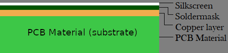
The single layer PCB is a very common type because they are easy to design and manufacture. One side of the base material (fiberglass, polyimide or metal) of this type of PCB is coated with a layer of a conducting material, usually copper since it has good electrical conducting properties. A layer of solder mask applied on top of the copper protects the PCB against oxidation and on top of that sits a layer of silkscreen which enables a clear marking out of all the components to the PCB.
Only one side of the PCB is used to connect different types of electrical components on a single-layer PCB. These kinds of PCBs are used in low cost, bulk manufacturing application like calculators, radio or printers.
Double-layer PCB
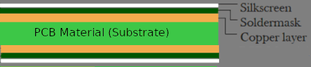
A double-layer PCB is a horizontally mirrored image of the single layer PCB with conductive, soldermask and silkscreen layers on both sides of the base material. The additional layout spacing provided by two conductive layers makes it suitable for most medium-complexity designs with components placed on both the top and bottom of the circuit board.
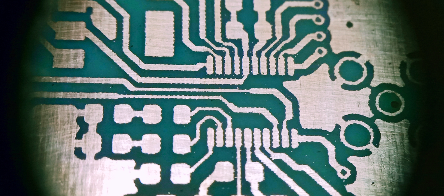
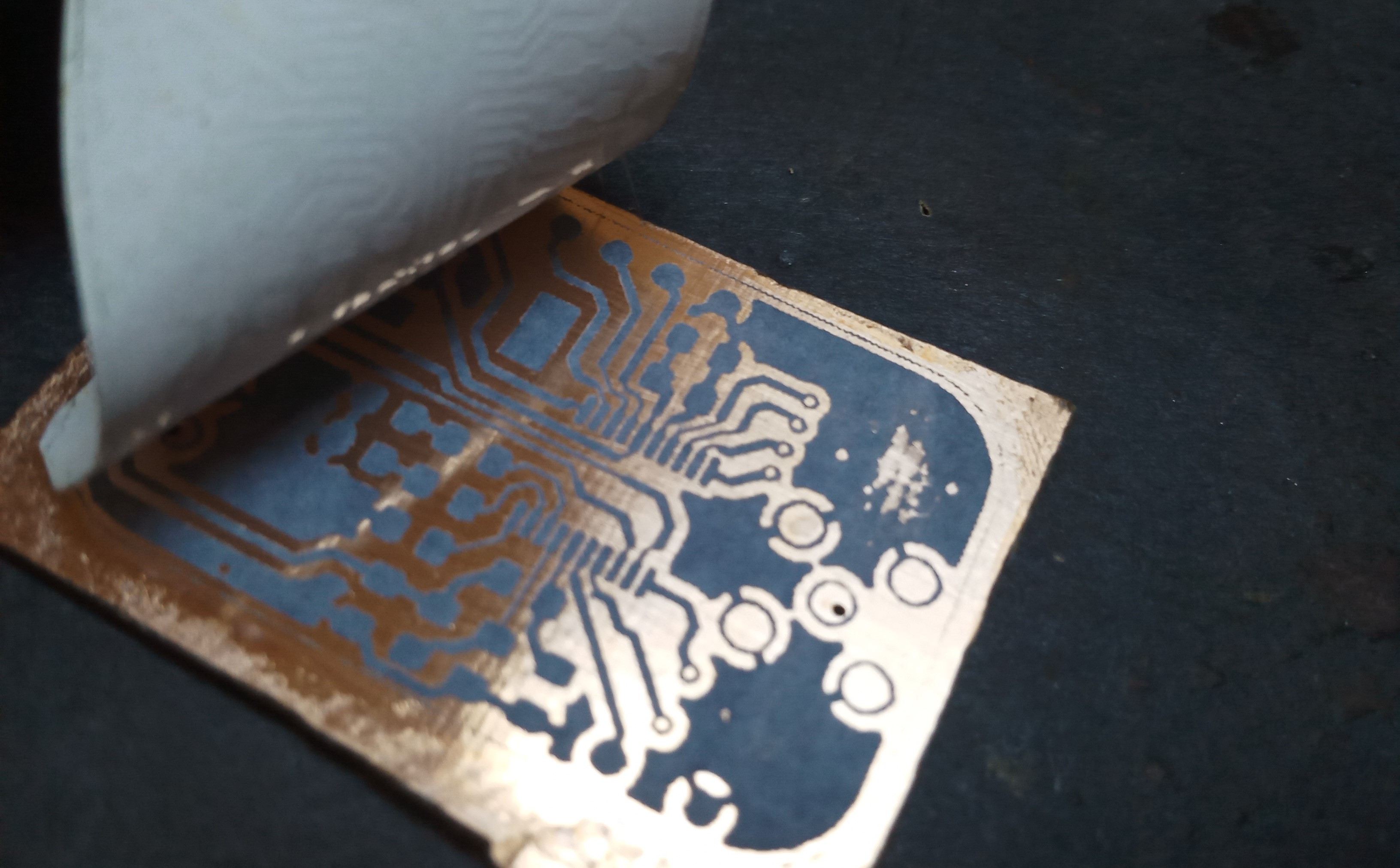
This is the type of PCB we’ll be making by toner transfer and etching. Here, toner from a laser-jet printer is transferred onto copper clad board by application of heat and covers the copper surface in the shape of the circuit to be created. When the board is the placed in a solution that dissolves (etches away) copper, the area protected by toner remains unetched and this is what will form connections between components.
Preparing the design
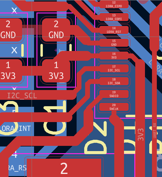
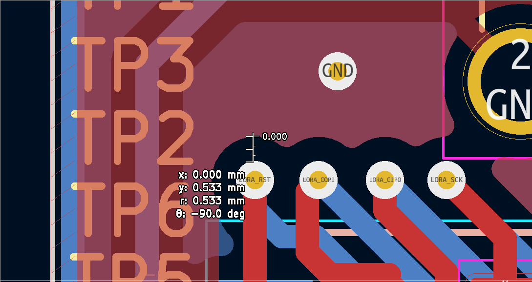
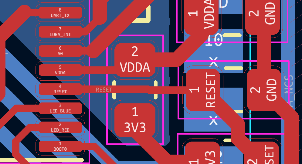
The particular circuit board is a LoRa communication dongle for PCs that can be used for free, point-to-point commuication and file transfer. It is based on an Ai-Thinker Ra-02 and an STM32F030F4 communicating with a PC over UART. All schematic and PCB design files are created in KiCad and are available on the project’s github repo. There are a number of adjustments that need to be made to leave a good enough margin of error to suit the fabrication process we’re going to use.
1.Track widths.
Keep tracks at a minimum width of 0.5mm, however if need be, you can use 0.25mm but as soon as it is possible, expand to 0.5mm tracks.
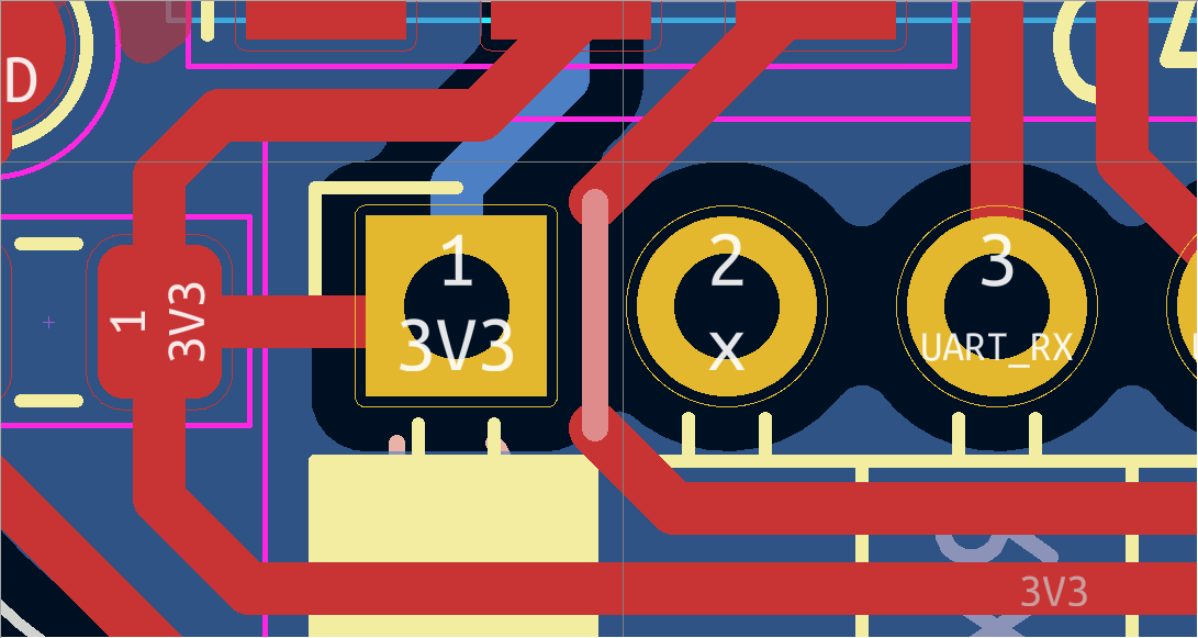
2. Clearances
A 0.508mm clearance between tracks, component footprints, vias and filled zones.
3. Component placement
Try to ensure tracks don’t cross into component courtyards, though this might not be a problem when soldering if you are skilled or patient enough; better yet, both.
Apart from these three tips, other standard PCB design guidelines - such as placing decoupling capacitors as close as possible to relevant device pins - still apply.
Conclusion
We’ve discussed the basic structure of a single and double layer PCB as well as the design considerations needed to make a design manufacturable using out home-made techniques. You can probably get away with using tighter tolerances with a little more patience and keenness, but I have found these dimensions to give consistent results in my trials. In the next part, we get our hands dirty with the fabrication process which will be quite engaging and equally more fun.
Comments