Homemade Printed Circuit Boards - Part2: Fabrication
In this second part of a three-part series detailing the process of creating a double-sided printed circuit board at home, we get down and dirty with the details of how a design is transformed into a physical implementation on a circuit board.
Requirements
Materials
- Copper Clad board
- Ferric Chloride (anhydrous Iron III Chloride) salt or solution
- Clean Water (tap water is ok)
- Matte paper laser printer printout (inkjet print simply will NOT do)
Tools
- Ironbox, preferrably not a steam iron.
- Hacksaw
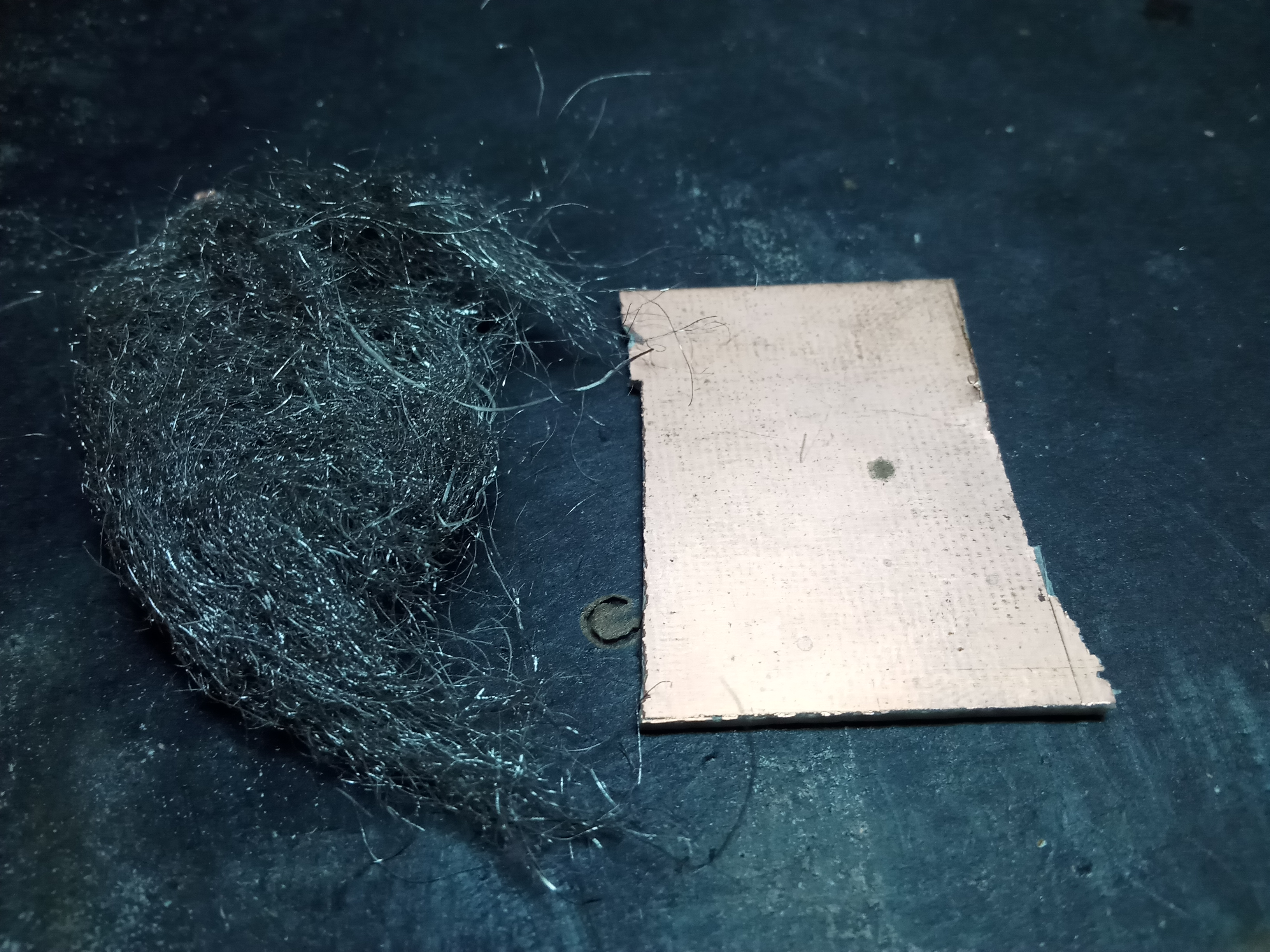
- Steelwool
- Paper tape
- Waterproof tape (Sellotape/duct tape)
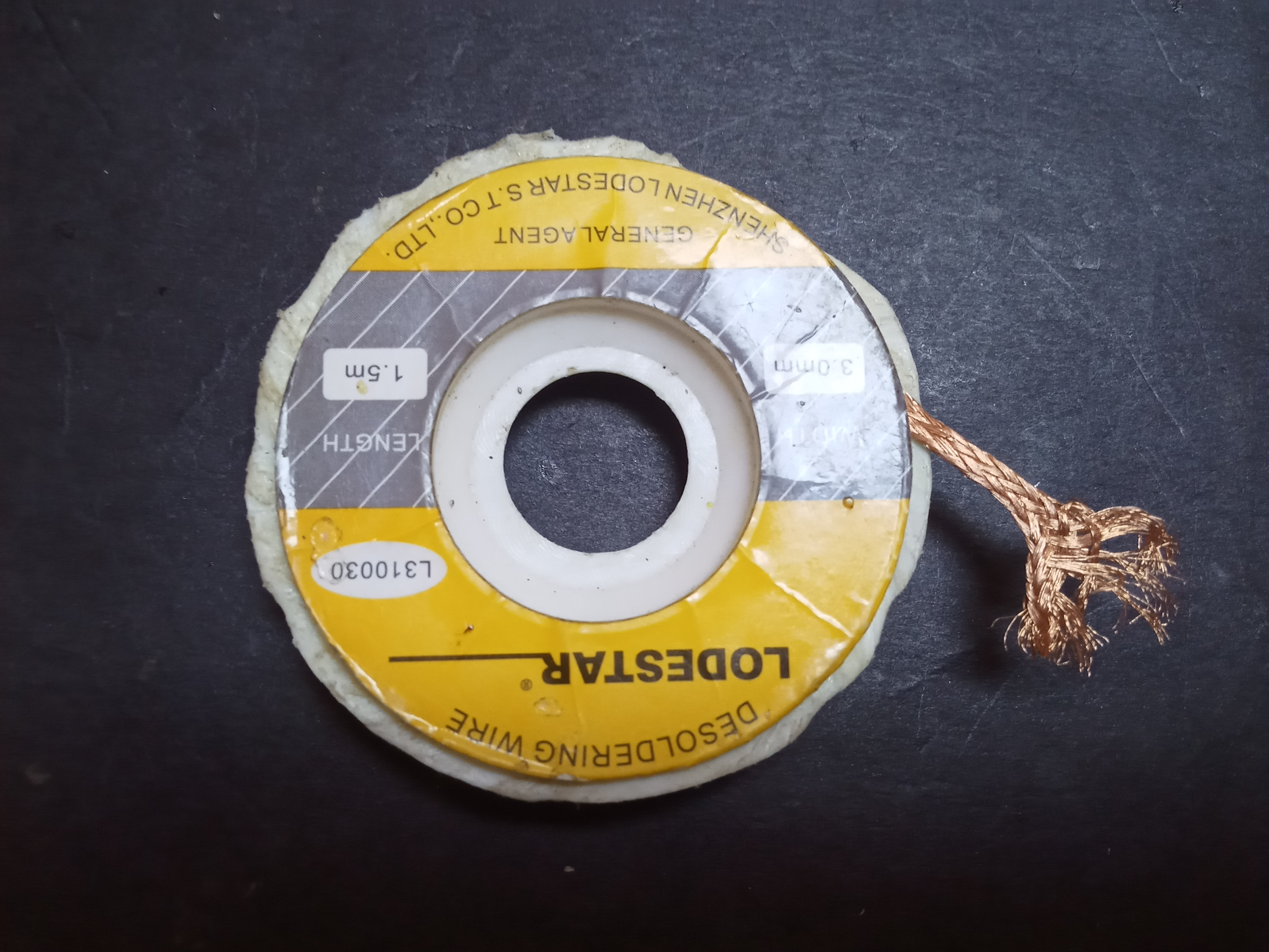
- Solder Wick
- Soldering iron
- Solder wire
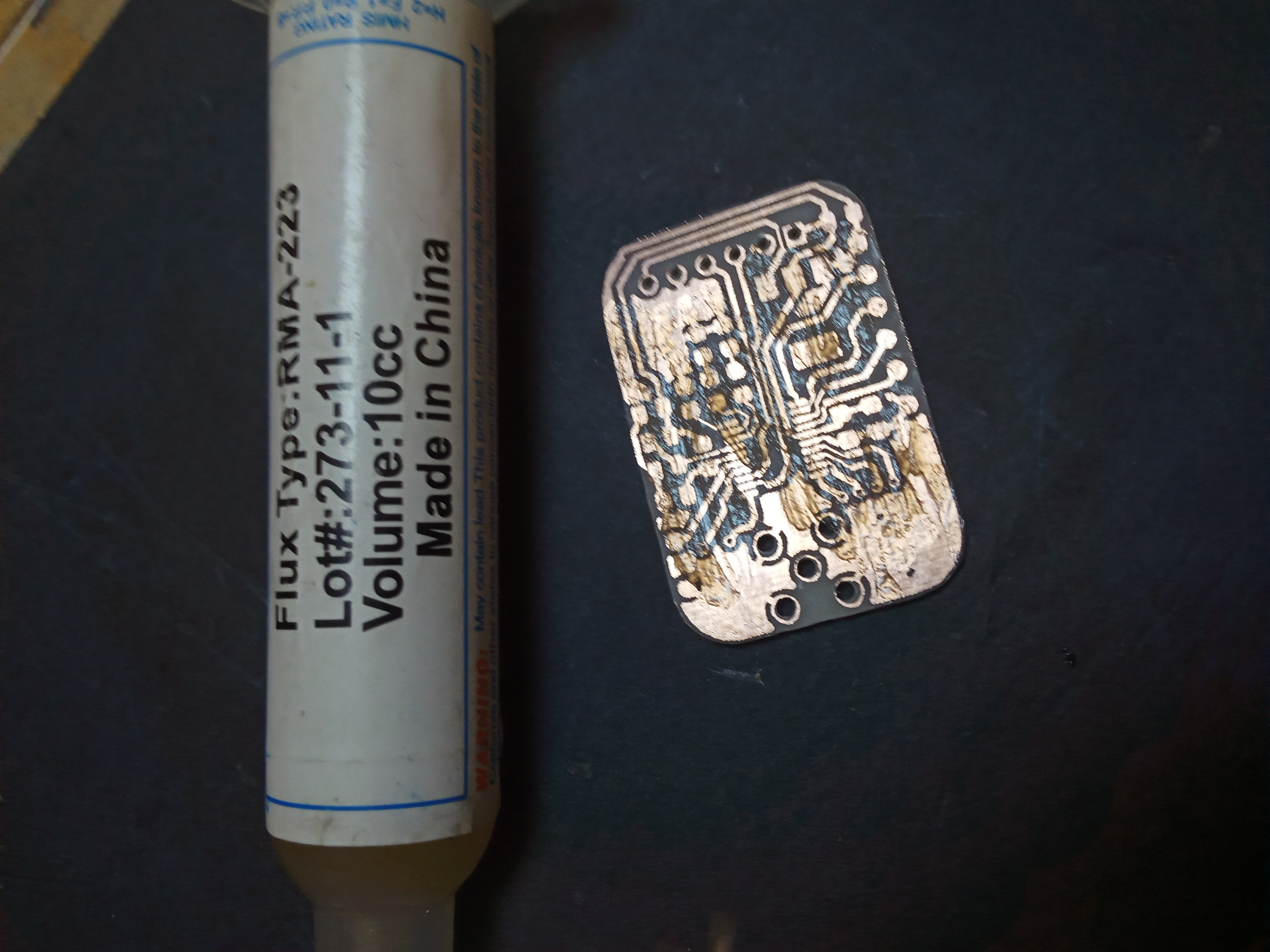
- Solder Flux
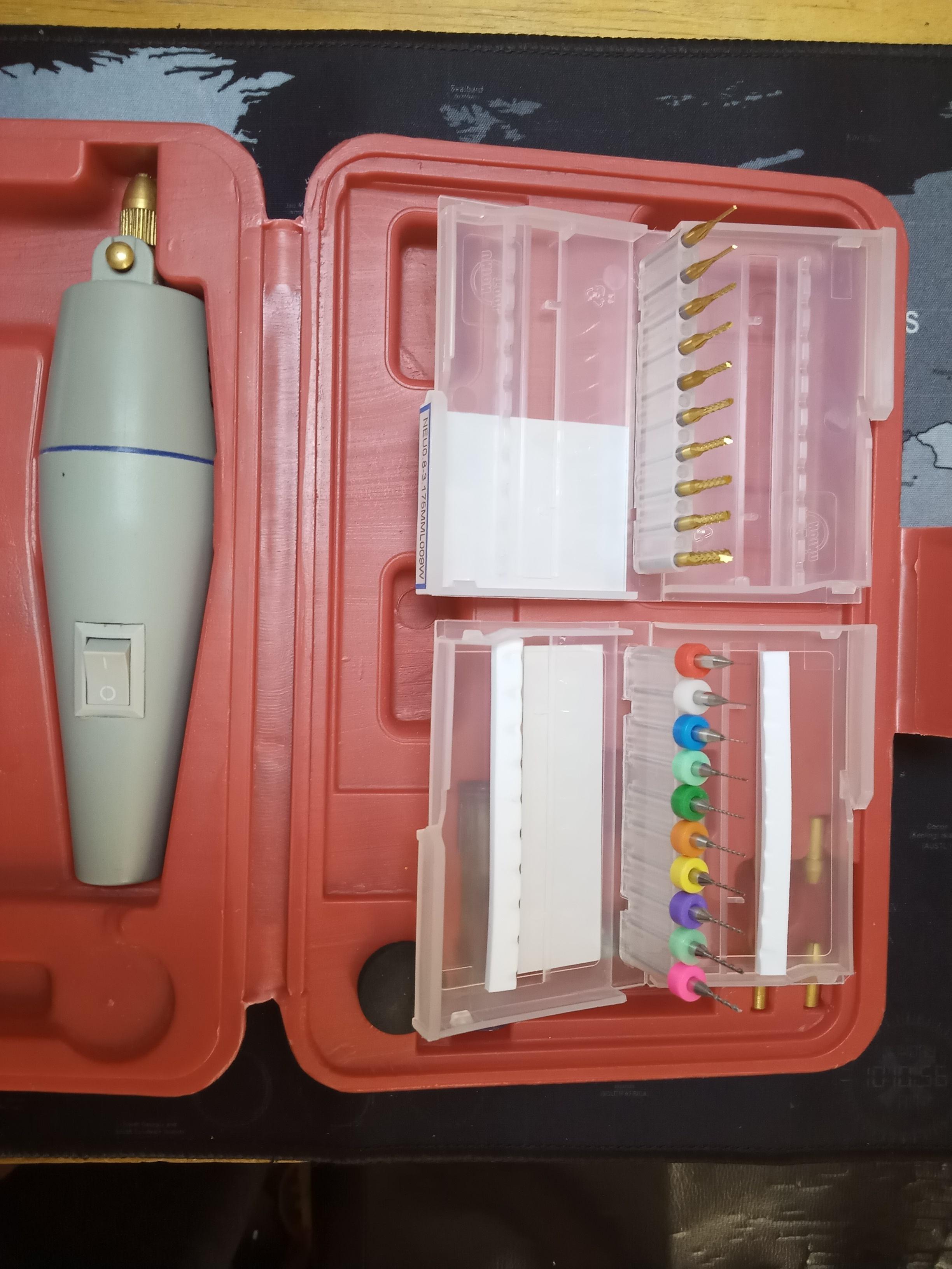
- Drill
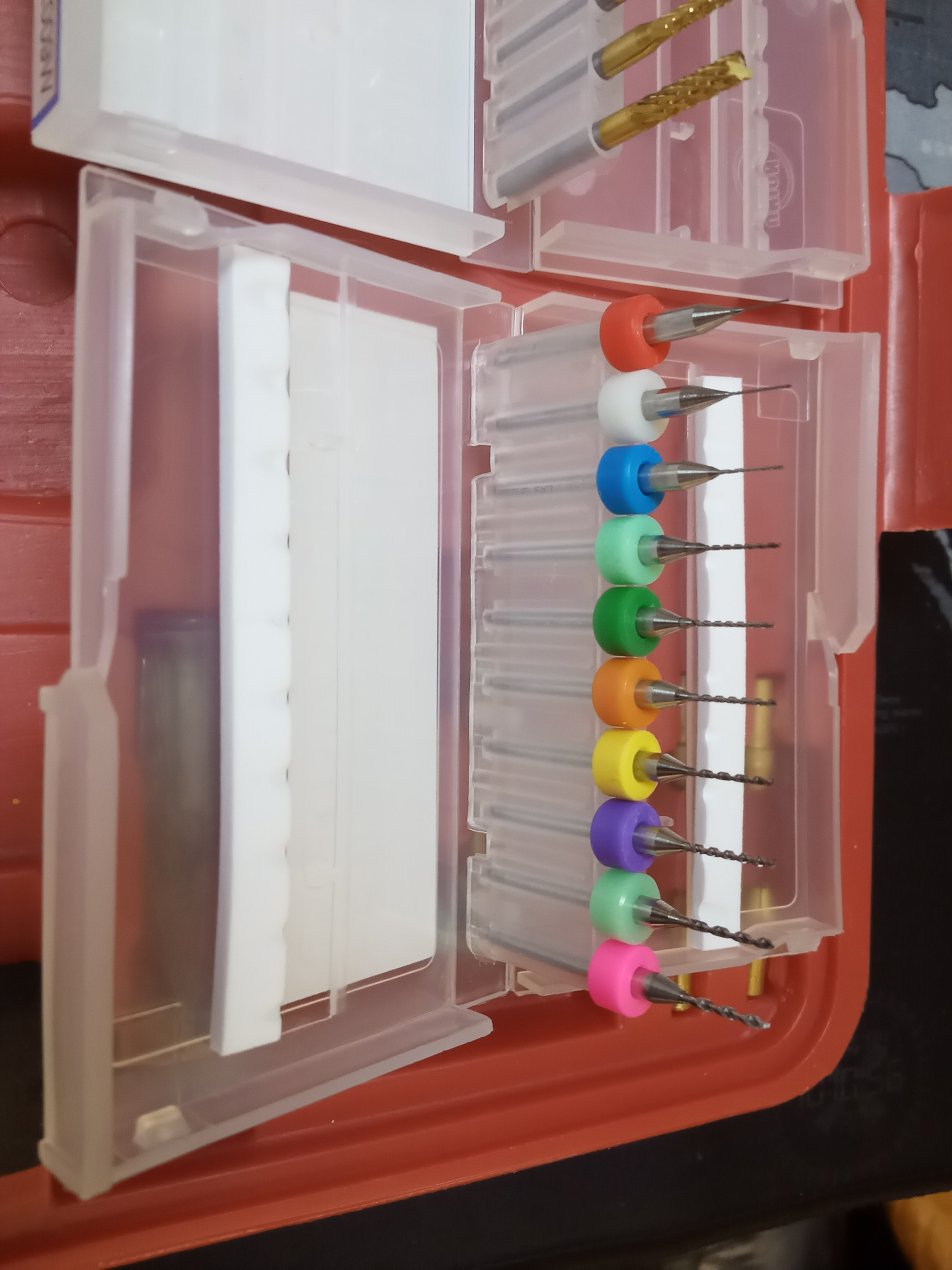
- Drill bits
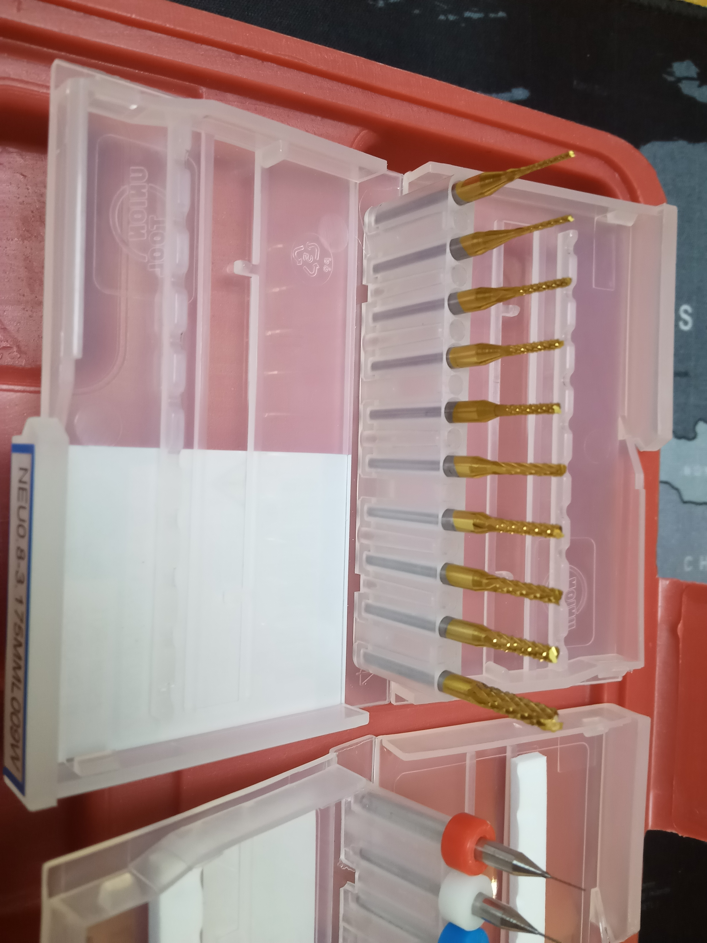
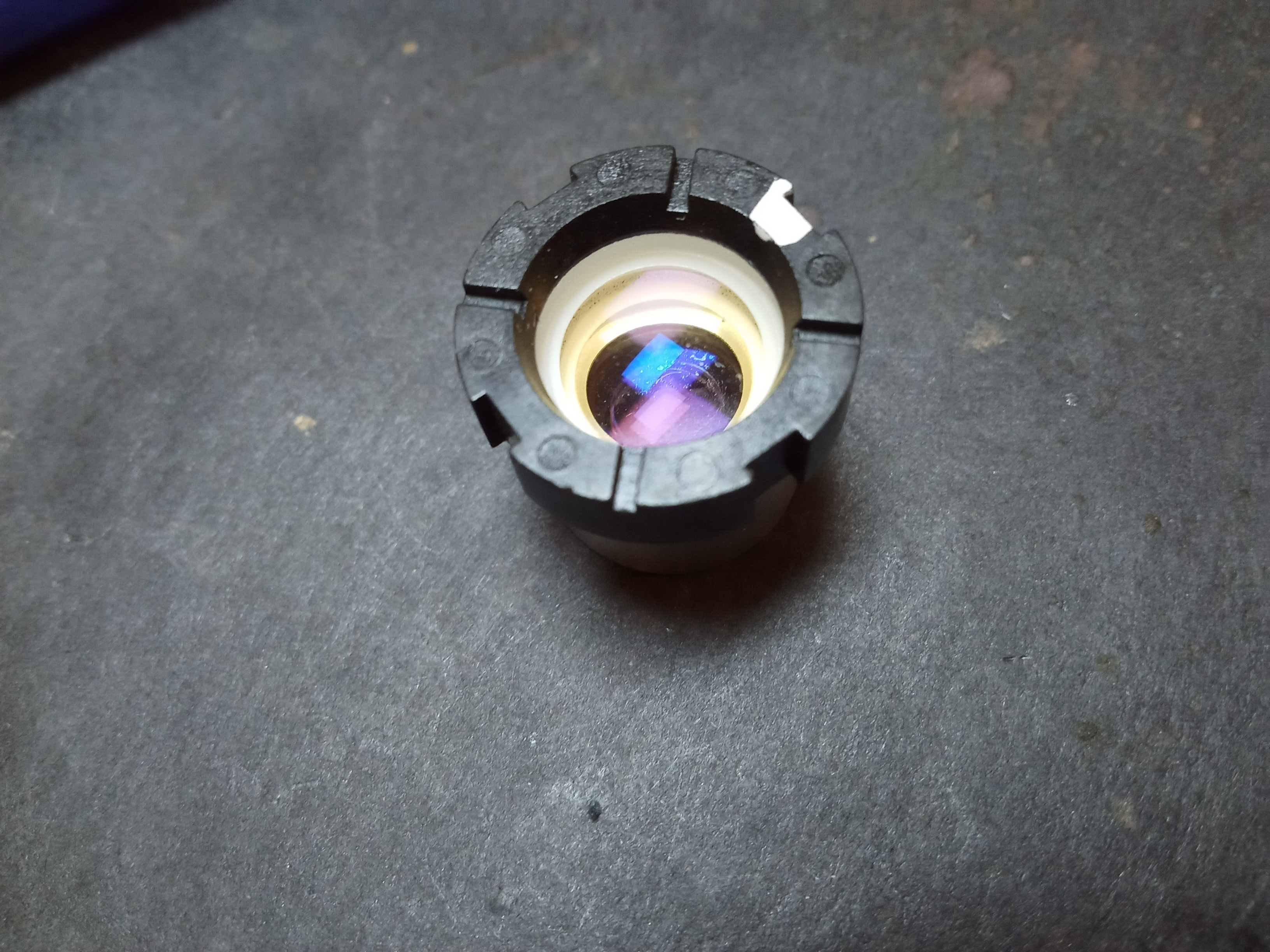
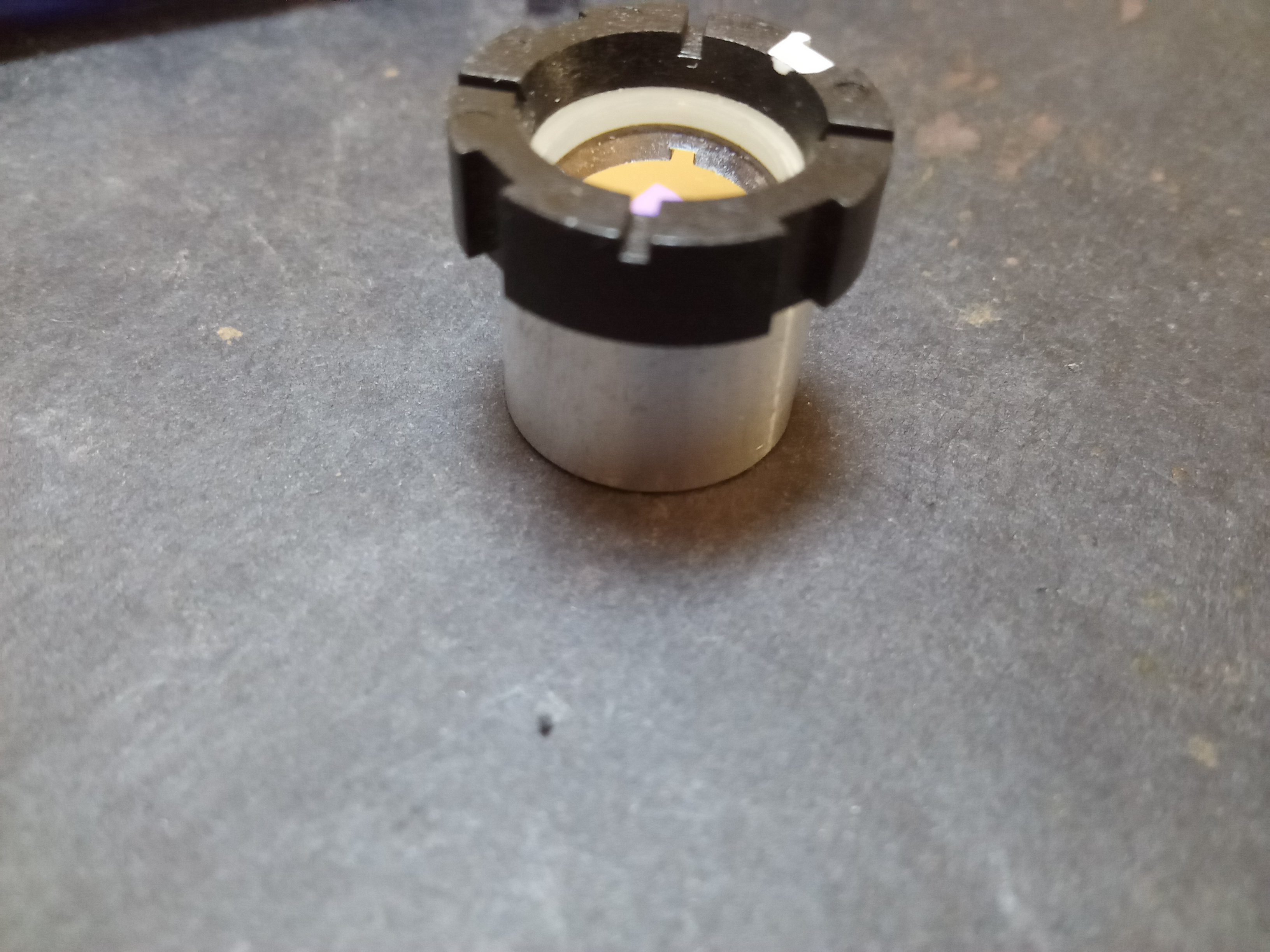
- Engraving bits
- Cotton wool
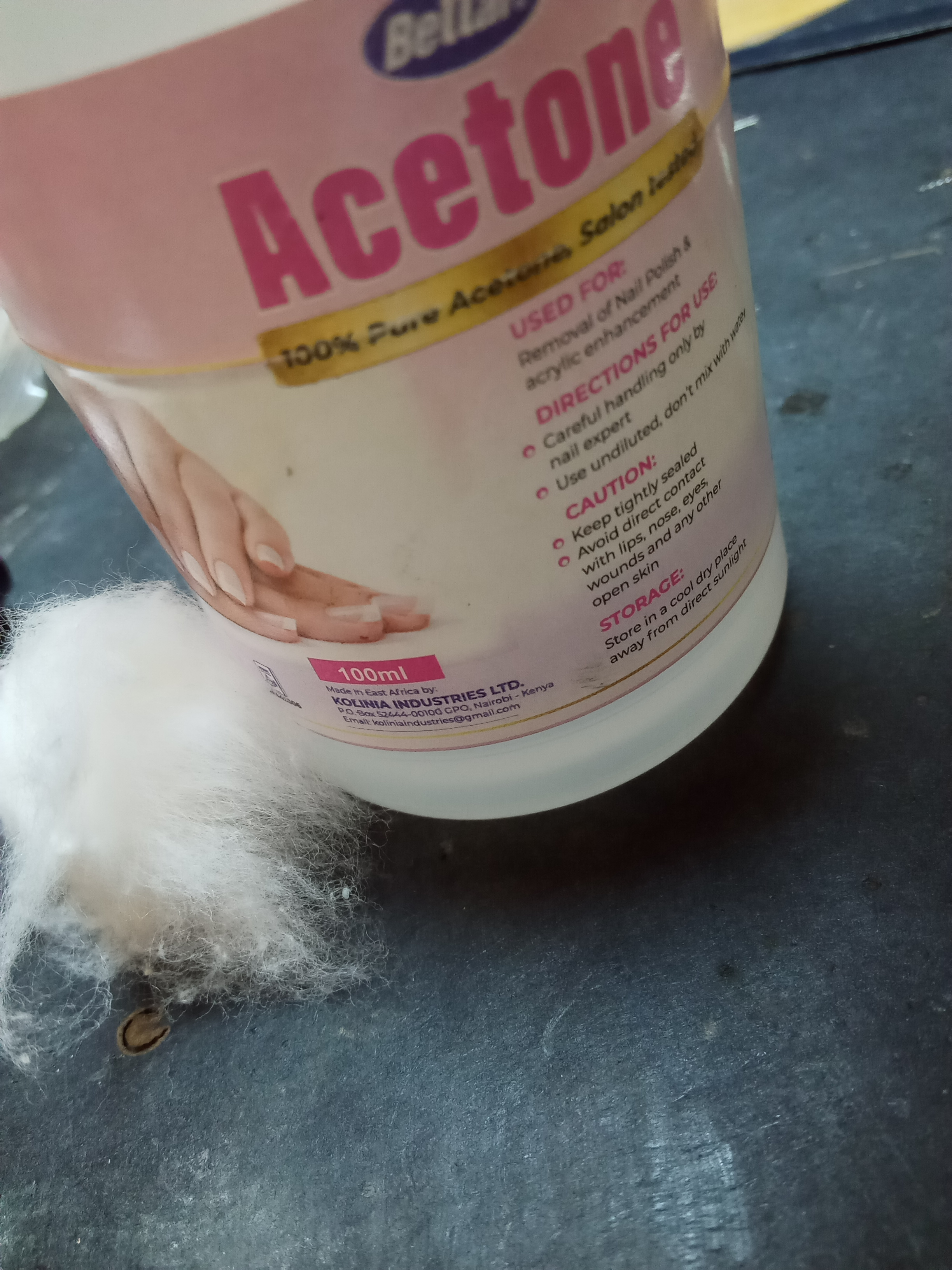
- Acetone
- A container large enough for your PCB to sit flat at the bottom
- Magnifying lens, for inspection
- Scalpel or razor
Software
- KiCad 6 and the PCB design files
Optional
- Inkscape (or any SVG editor)
Procedure
1. Exporting PCB printout from KiCad
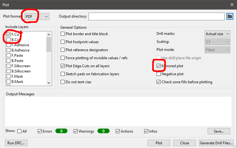
Open the PCB design files in KiCad and select Plot.
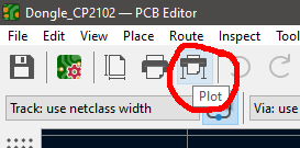
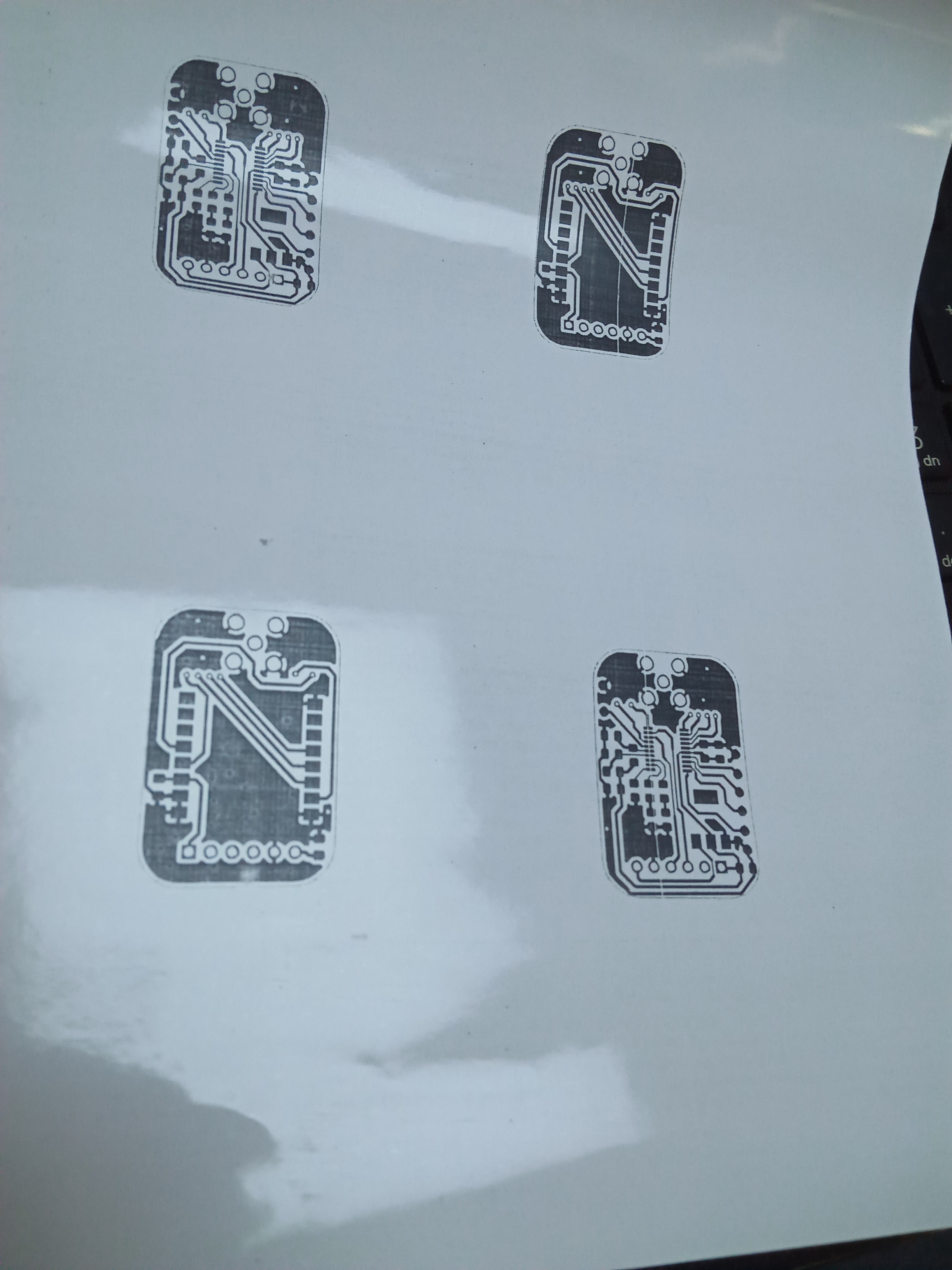
We shall export the PCB layers in PDF format for printing. Among the included layers, select Front copper (F.Cu) only and have the rest of the options as shown. Note that we check the Mirrored Plot option because the top layer appears mirrored when we do toner transfer on to the board. Then choose the directory where you want your PDF to be saved and click plot. The default location is the folder containing the PCB design files you are exporting.
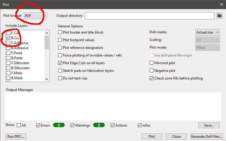
The setup is the same for the Bottom layer (B.Cu) except that we dont mirror it. Once you have all options as shown, click Plot.
Tip:
-
It may be necessary to print several copies of your pcb design at different locations on the paper in case your printer has uneven toner distribution, then there is going to be at least one good printout.
-
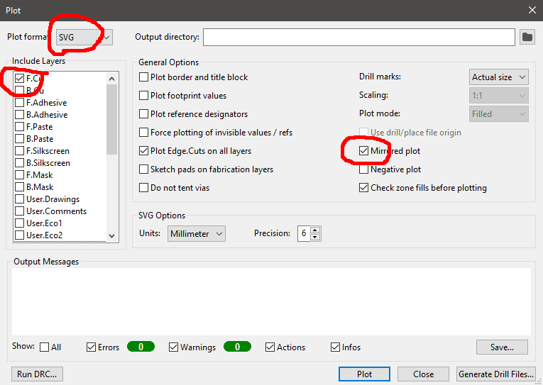
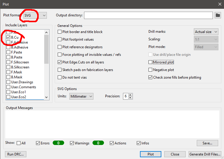
Sometimes the printout appears smaller or larger when matched up against the actual the components to be mounted. In this case, you will need to play around with scaling till you find what works for you. I have found that the best way is to export as SVG instead of directly as PDF, open the scalable vector graphic in Inkscape, adjust scaling as necessary and then export as PDF
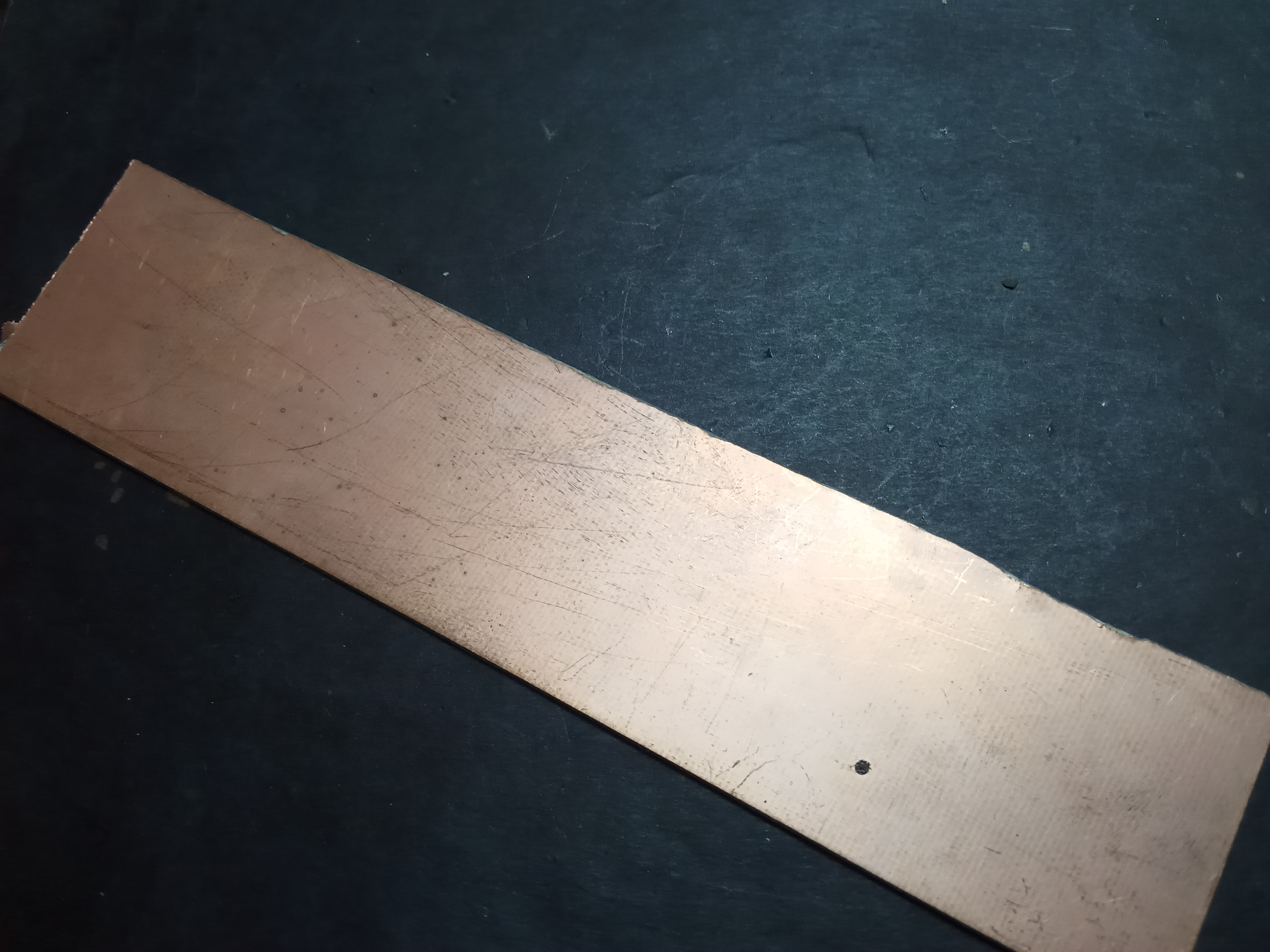
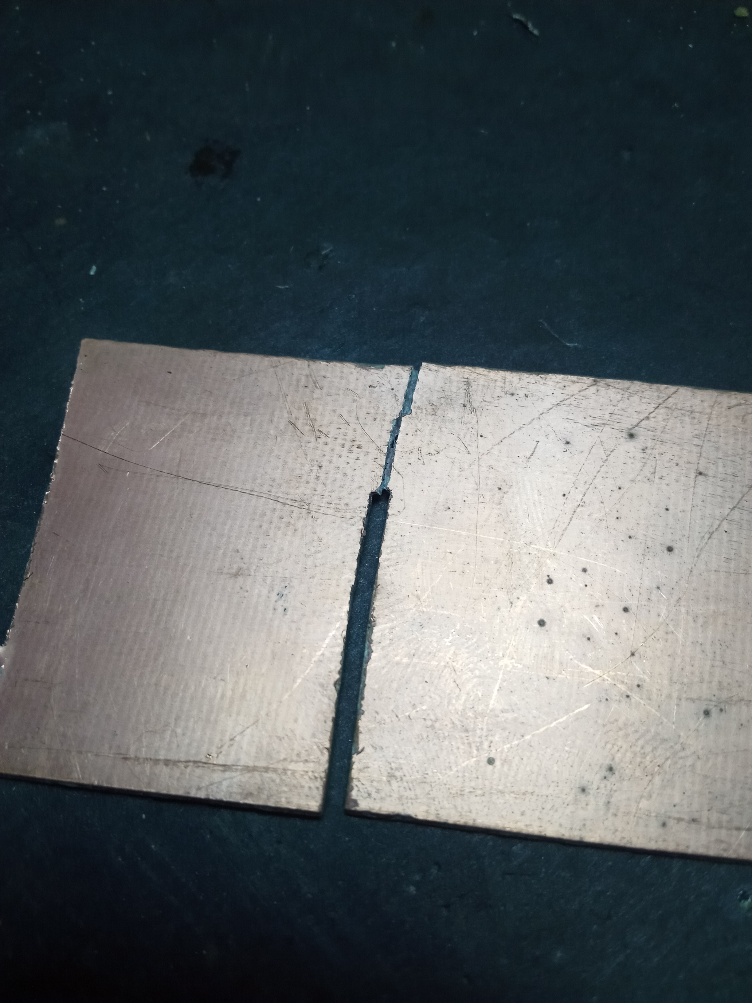
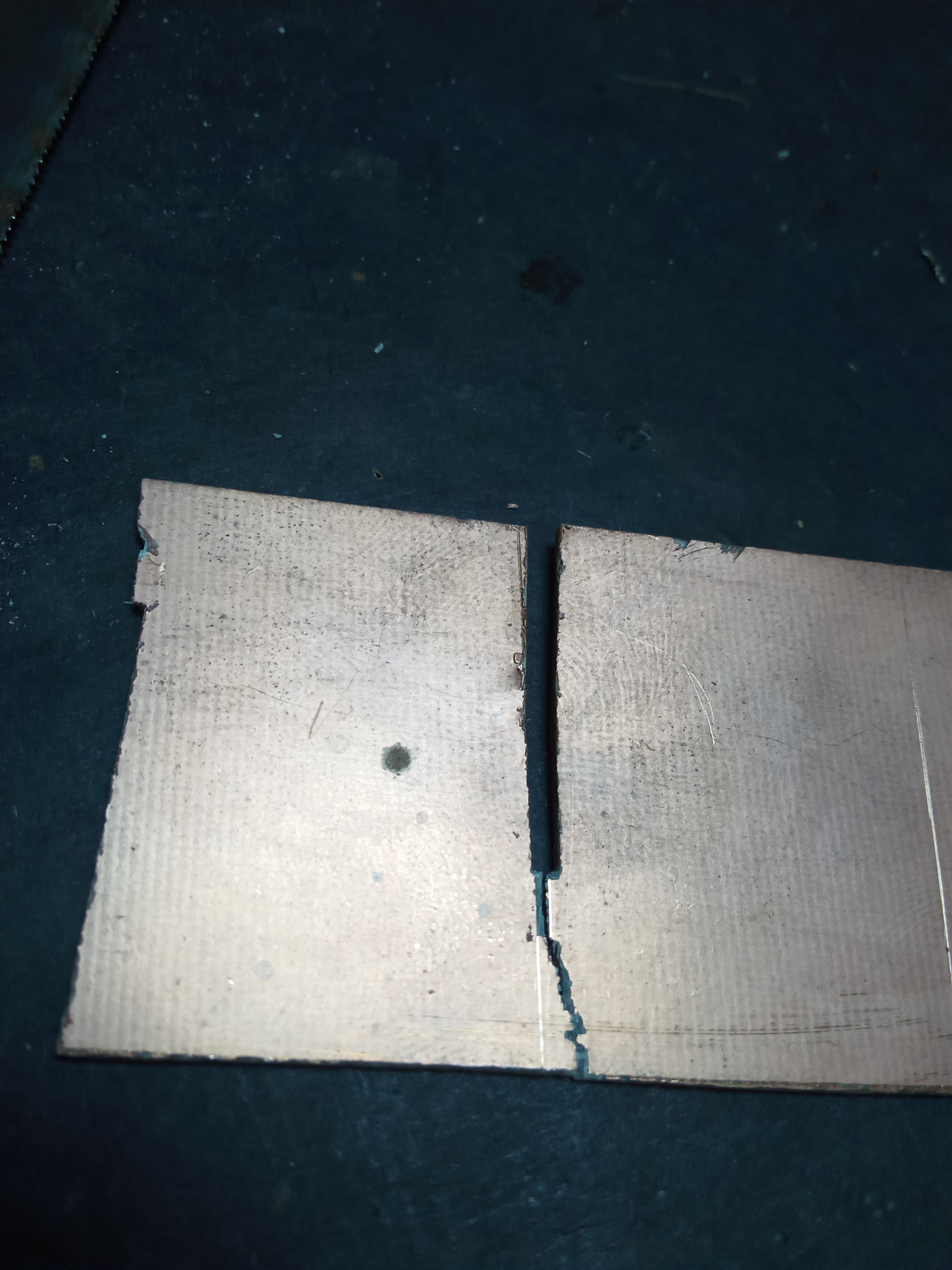
2. Cutting Copper Clad board
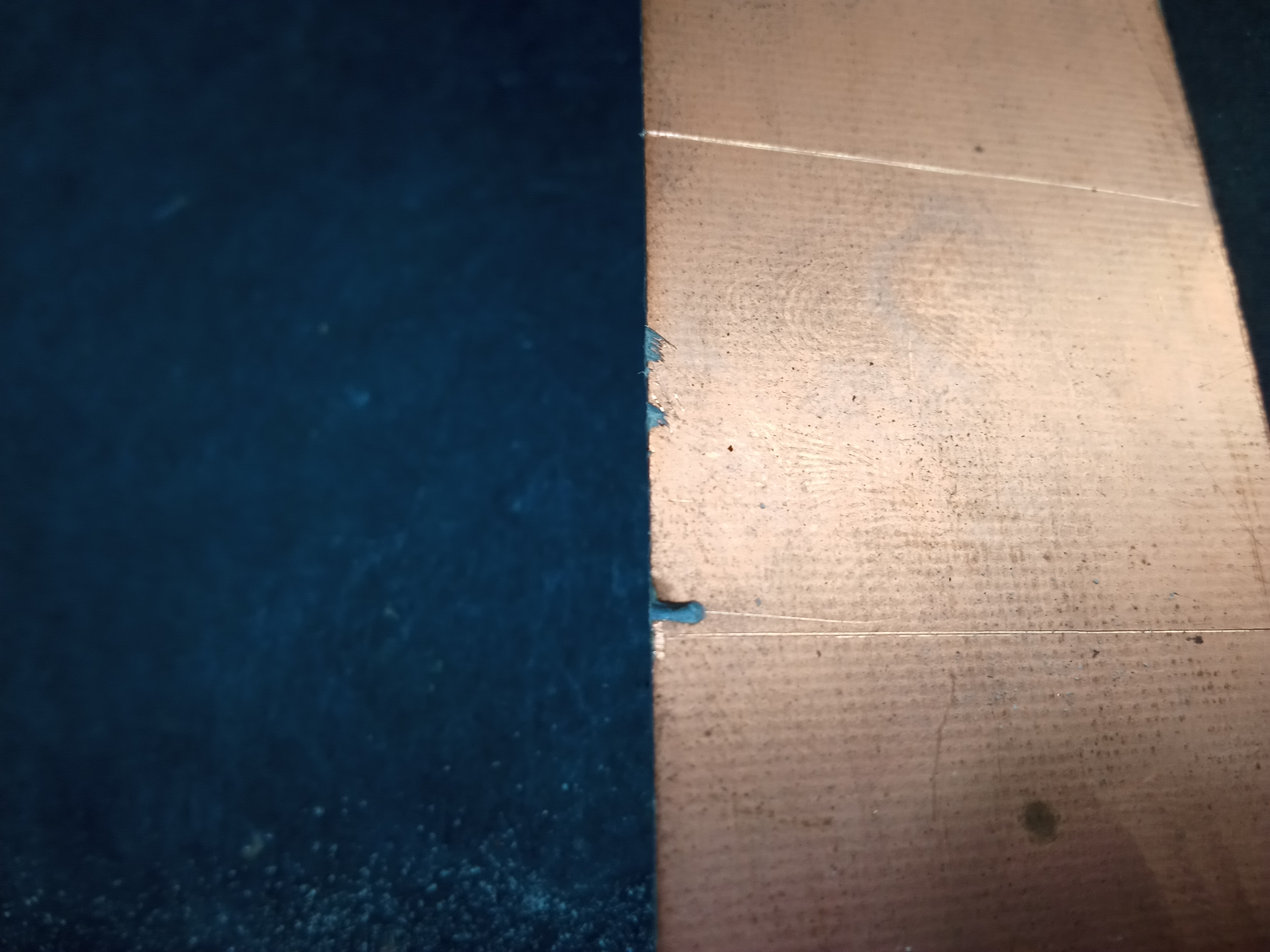
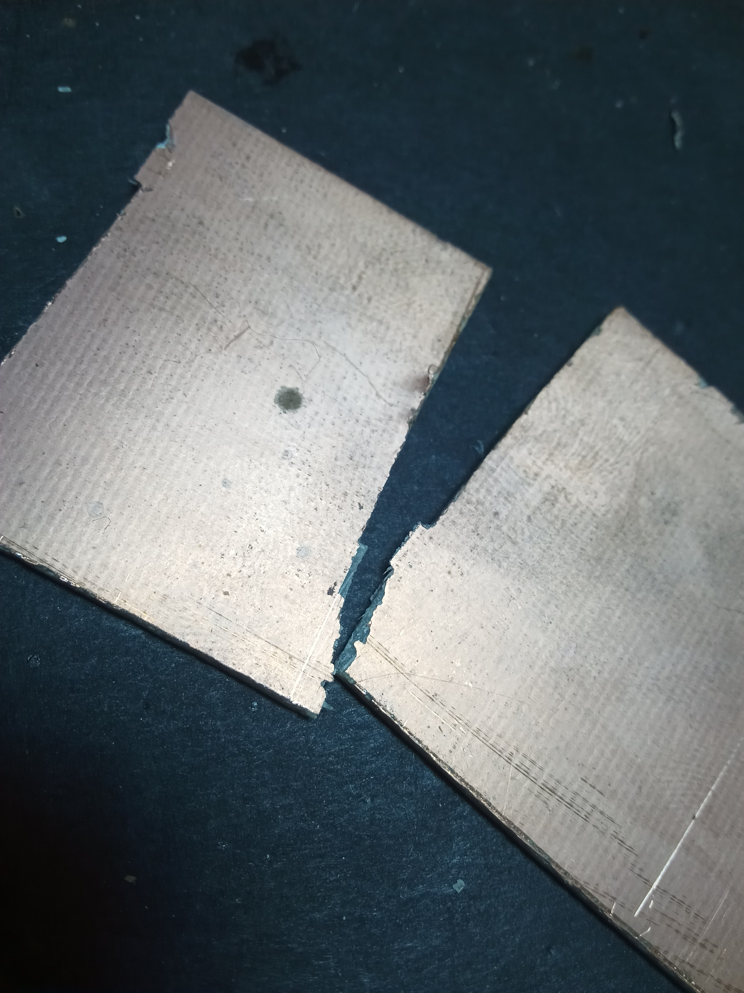
Cut the matte paper down to size leaving about a millimeter margin around your design. Lay the cutout against your copper clad board and scour its outline against the board - to create a guideline that will be useful while cuttong cutting - leaving a margin of a few milimeters to compensate for the width of the cutting blade.
Create a notch where you want to start cutting by runnung the hacksaw a few times in the direction opposite to that of its teeth. This makes for a far smoother start before the teeth begin to bite into the board.
You can now resume normal cutting with only one cutting stroke in the direction that the hacksaw teeth are facing.
Tip:
-
If using a standalone hacksaw blade, try to keep the blade perpendicular too the board to it does not get caught and bend. Otherwise, it will peel the copper off your board
-
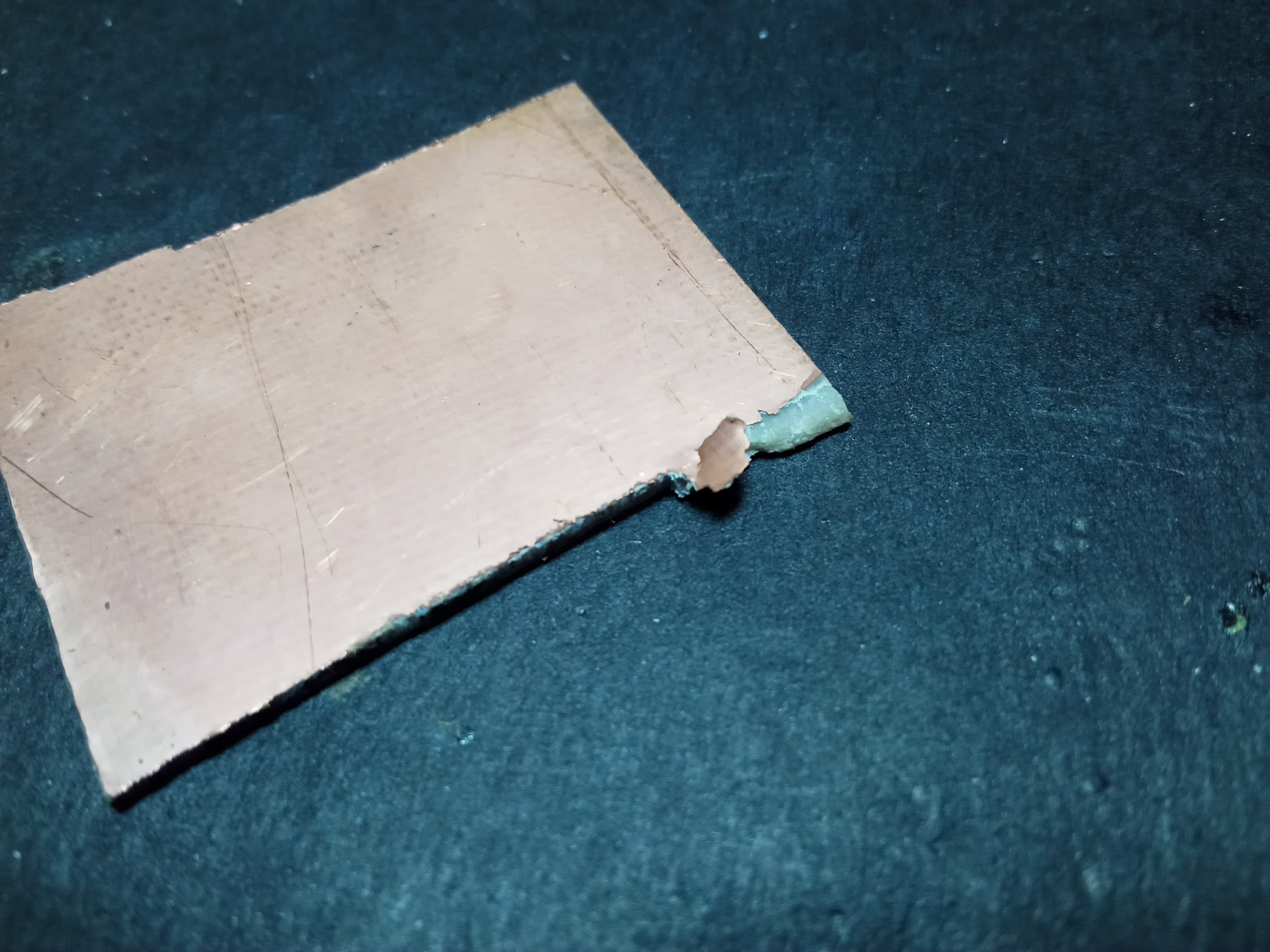
While cutting, be careful not to apply any shear (tearing) force on the board as it may break and likely peel away copper from the surface around the fracture. Be especially wary of this when the cut is almost all the way through the board.
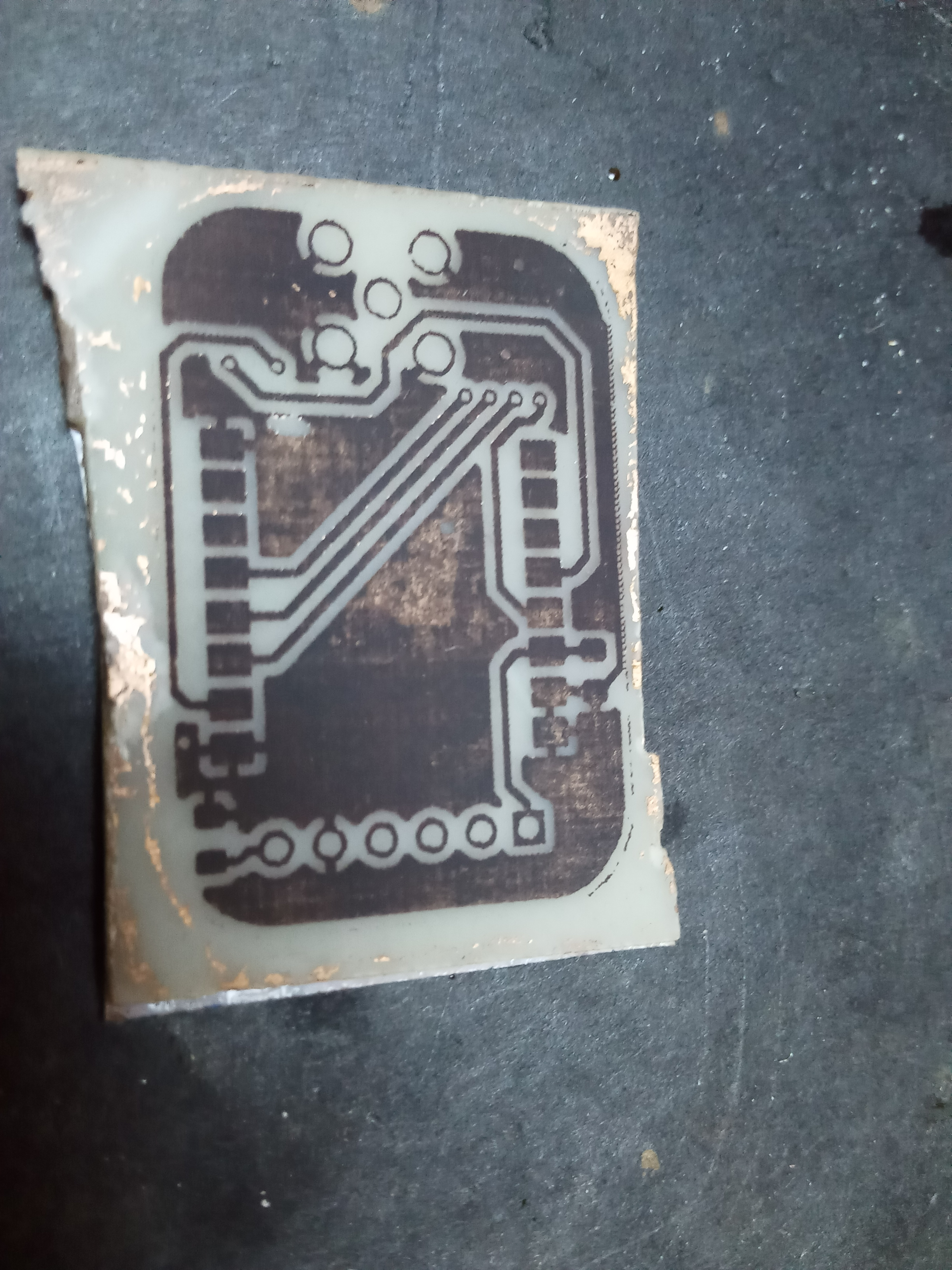
Top Layer Toner Transfer
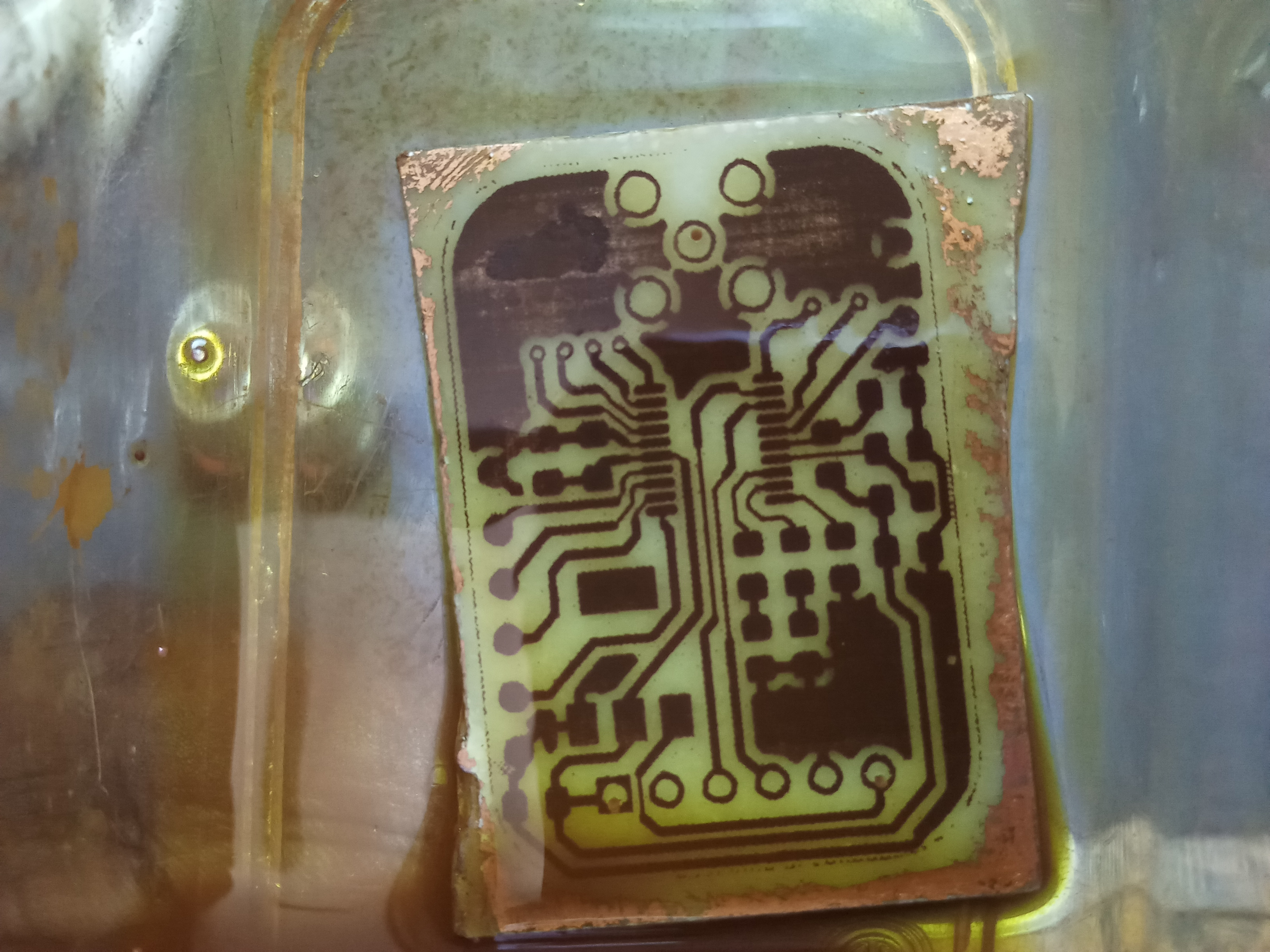
Having confirmed your matte paper cutout will fit well on the copper board we just trimmed down, scrub the copper to a lustre on the side of the board you plan to have as your top side. I have found a better finish using a linear scrubbing motion as opposed to a circular one.
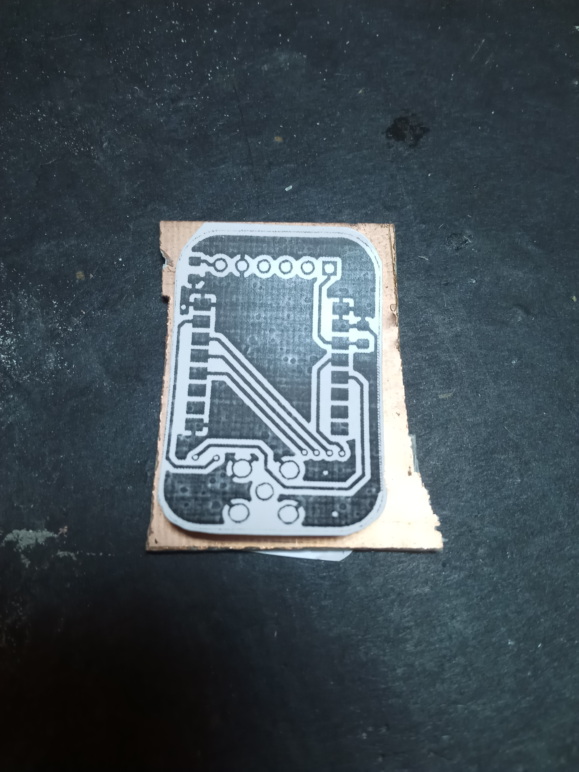
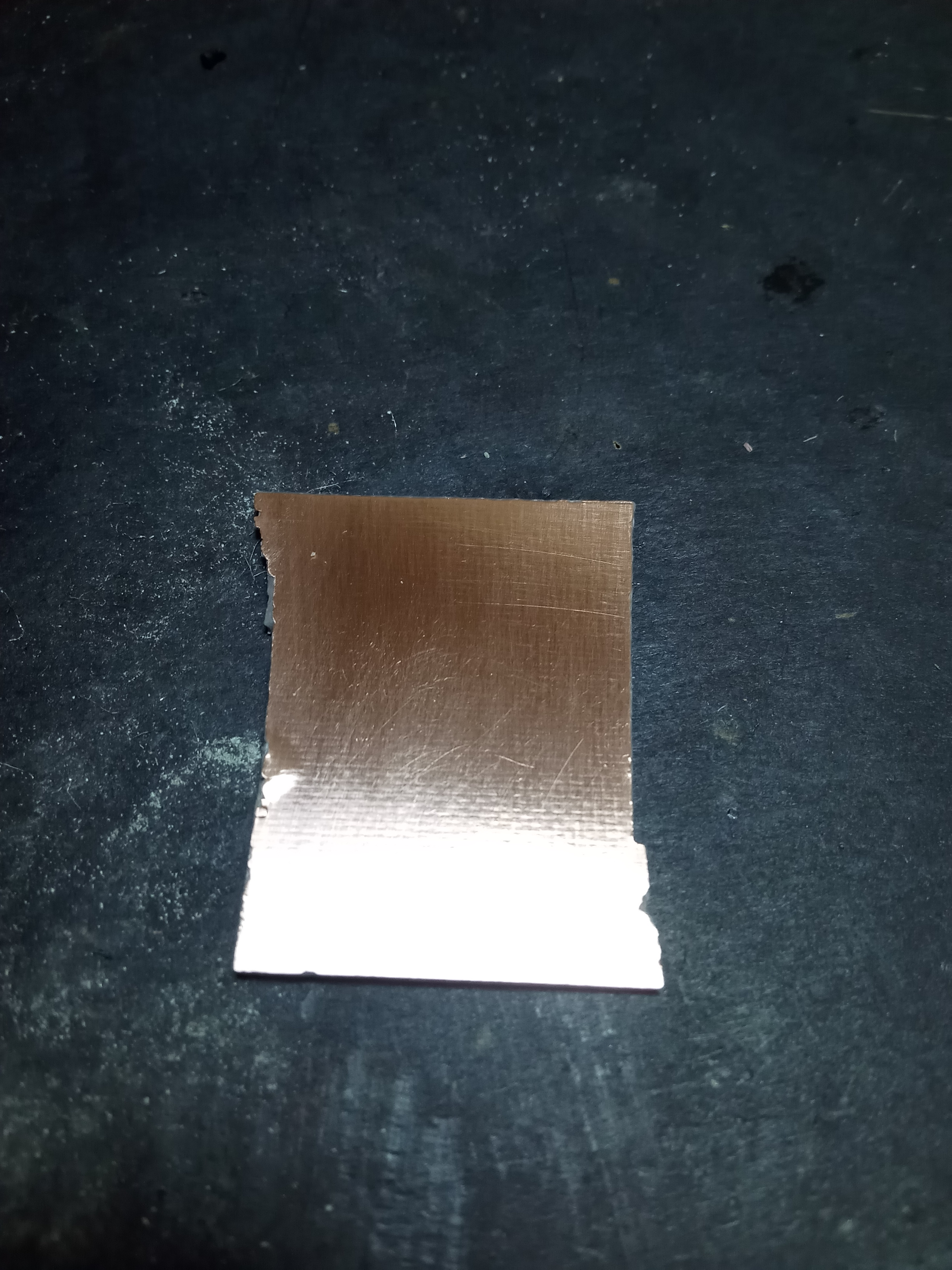
Place the cutout face-down on the lustrous side of the board and tape over it with paper tape. Paper tape stands up to the heat much better than other types of tape.
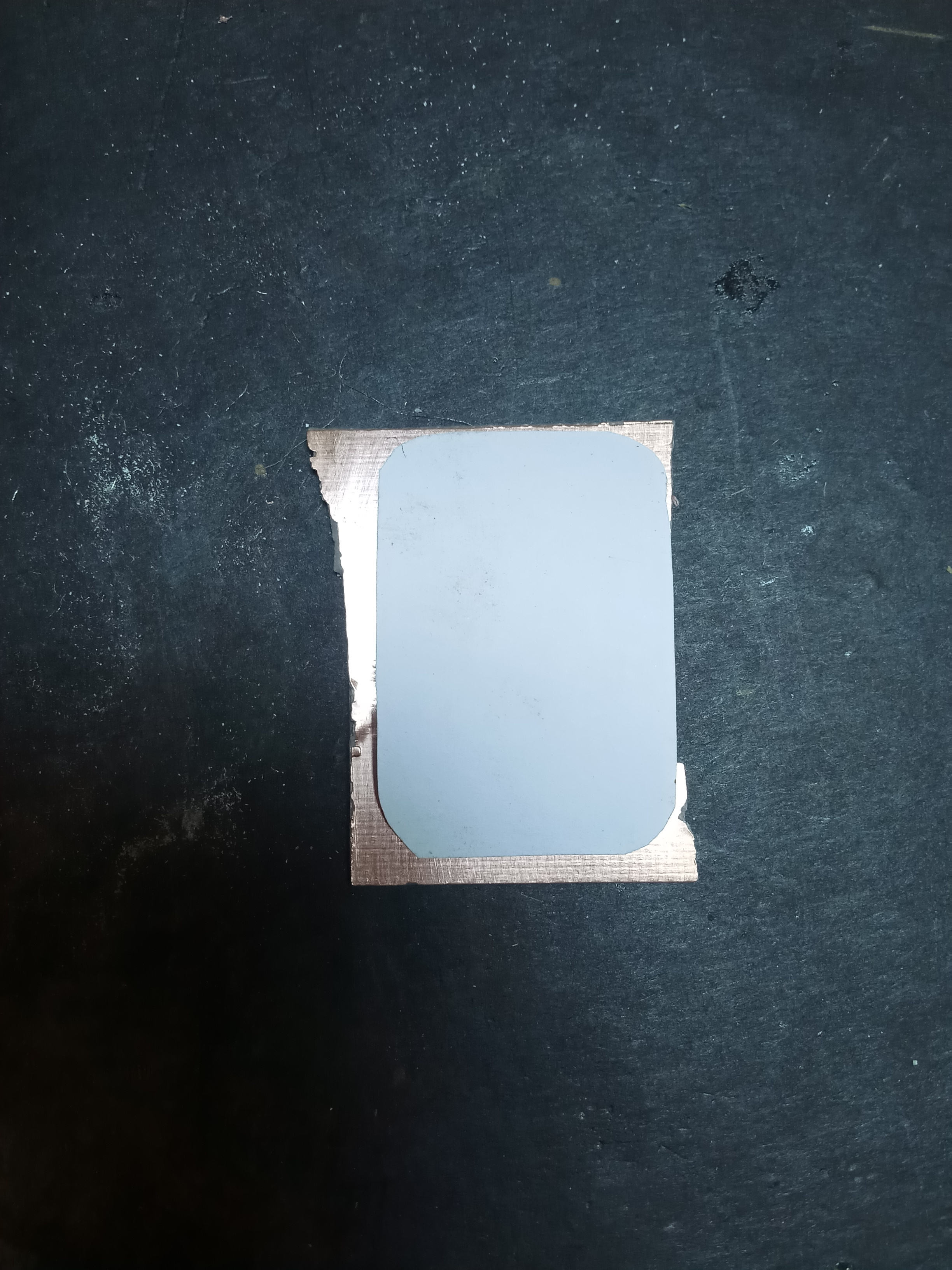
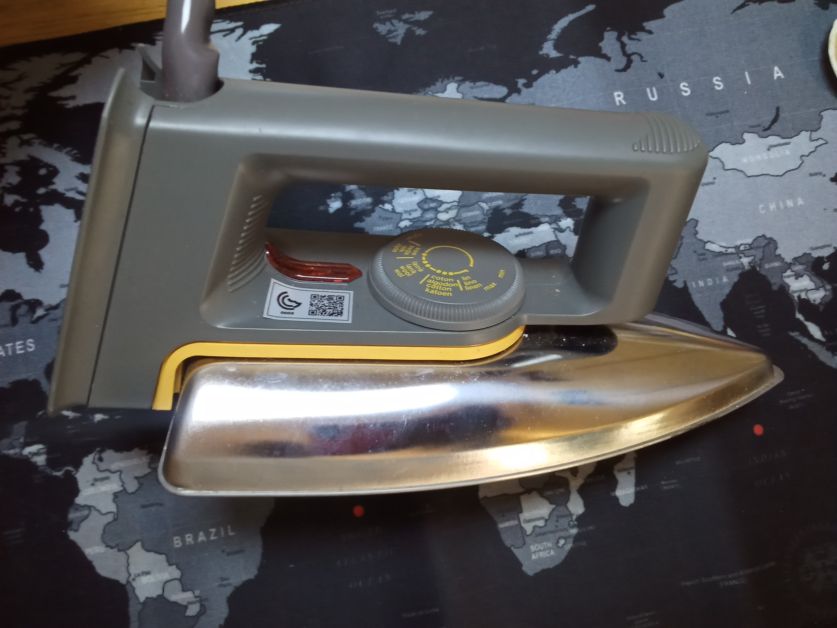
Set your iron box to maximum setting and allow it to heat uptill the thermostat kicks in. Ideally, you want an ironing surface that is smooth, flat and resistant to heat; I use concrete. Iron over the cutout for 5 - 10 minutes, applying pressure while moving the iron box around to even out the heat distribution. You will know the PCB is ready when the matte paper begins to turn black under the tape, but feel free to continue until your gut says it is ready. At this point the PCB is still hot to the touch so give it some time to cool down as you sip some coffe; we still have quite a ways to go.
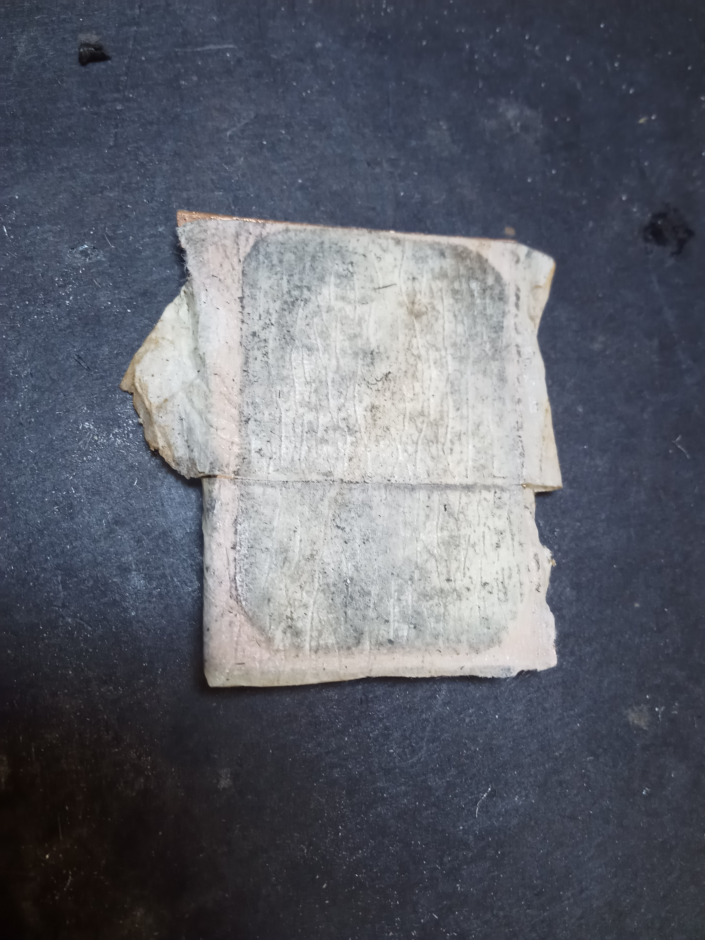
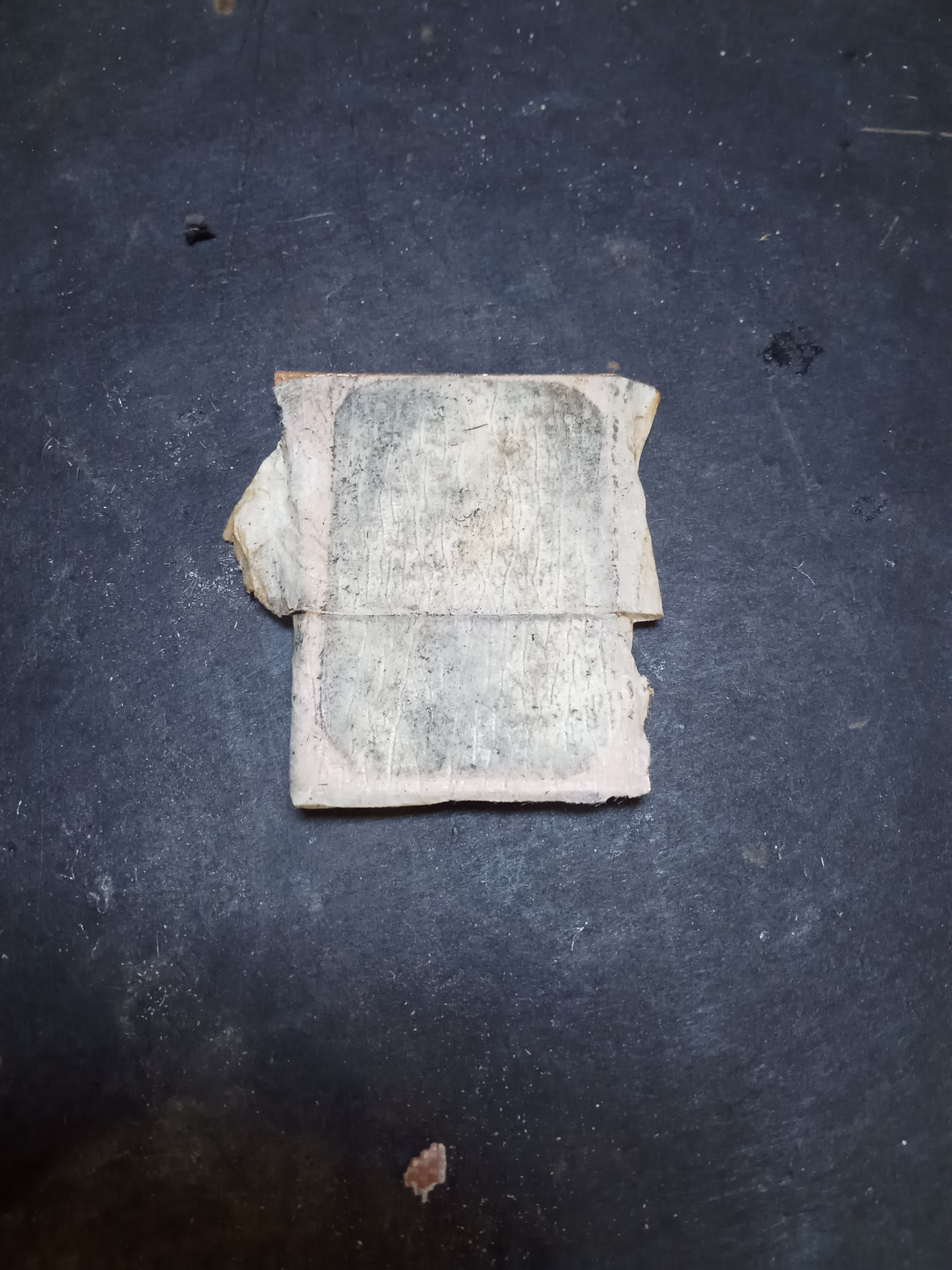
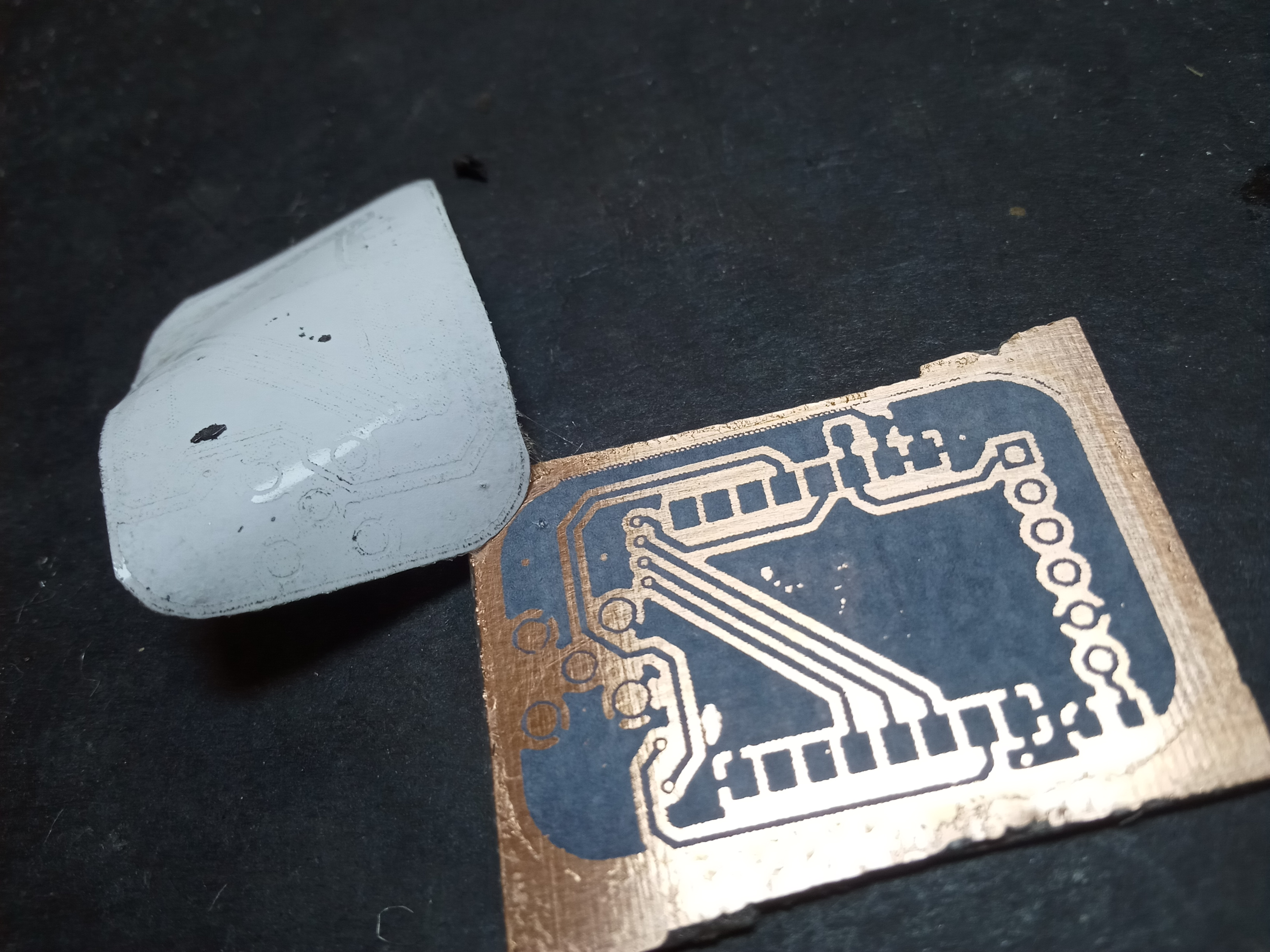
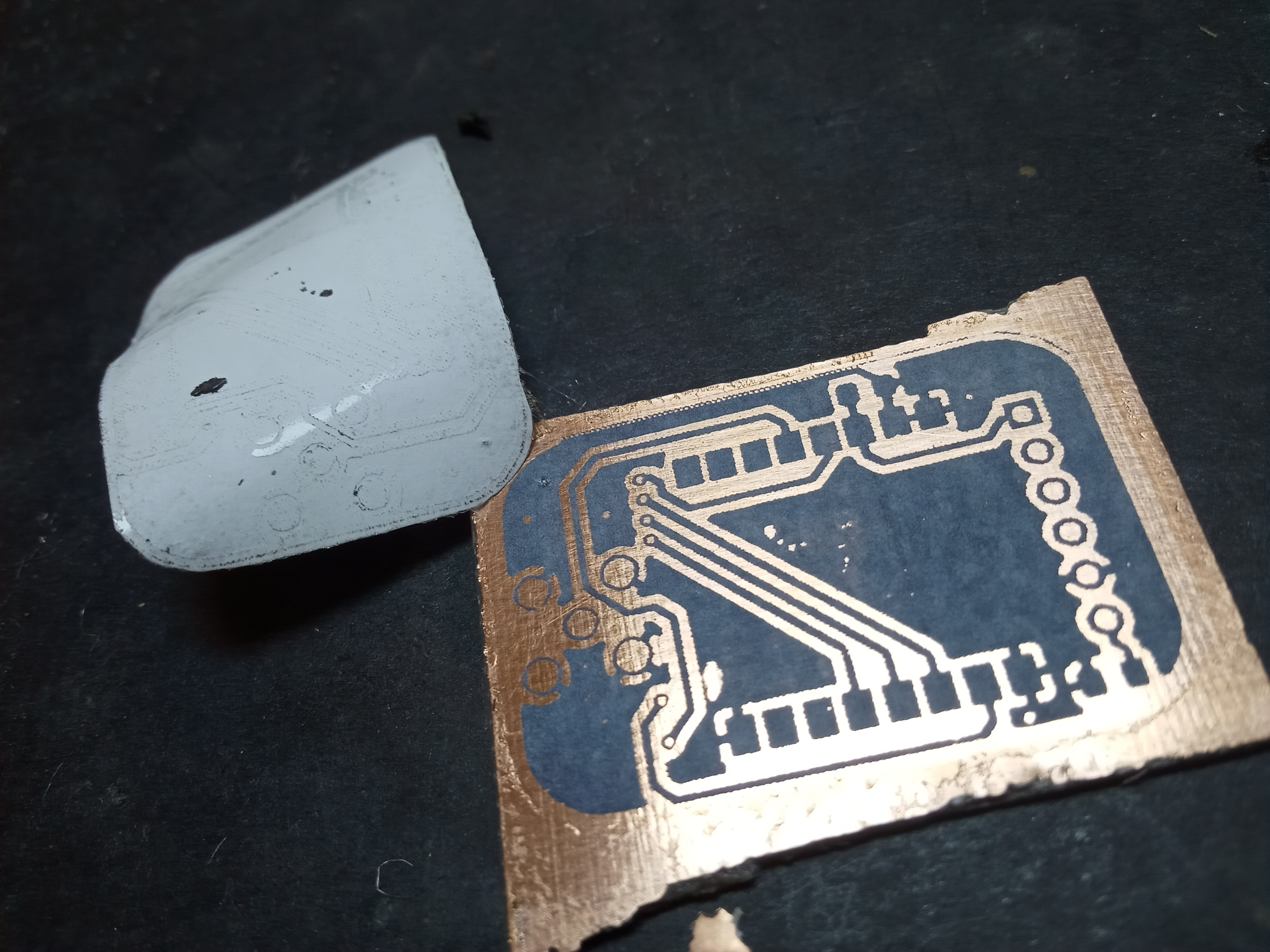
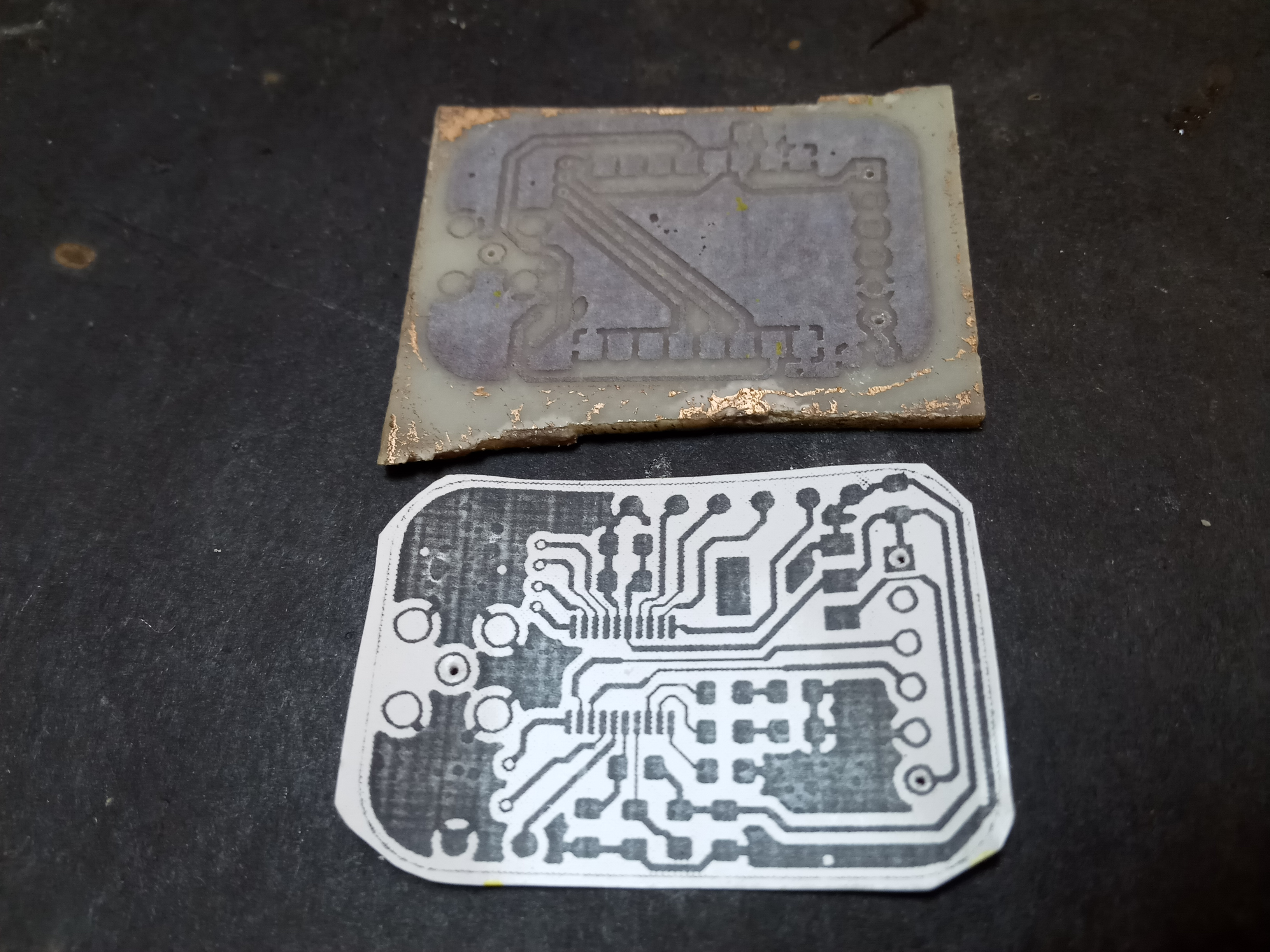
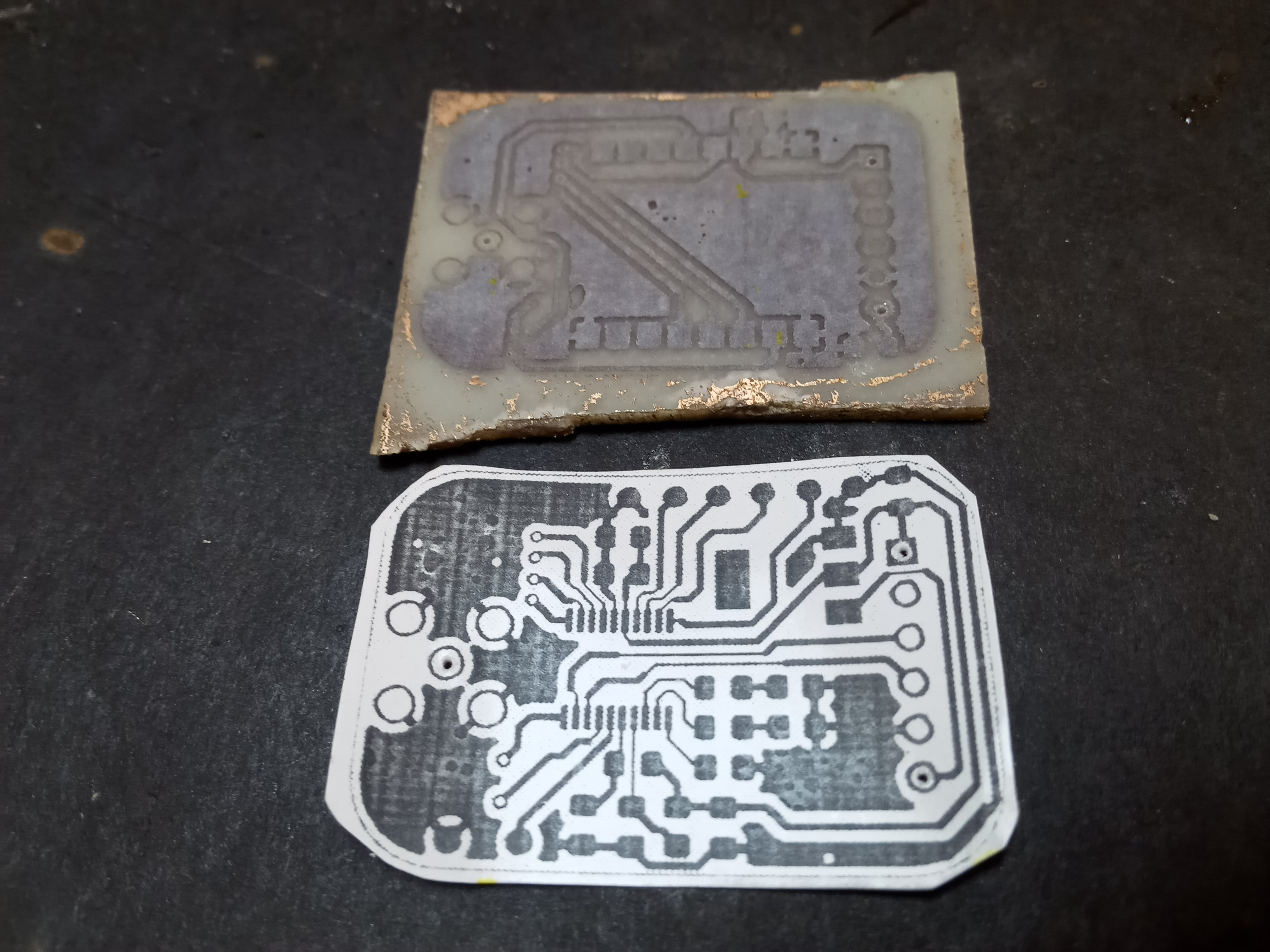
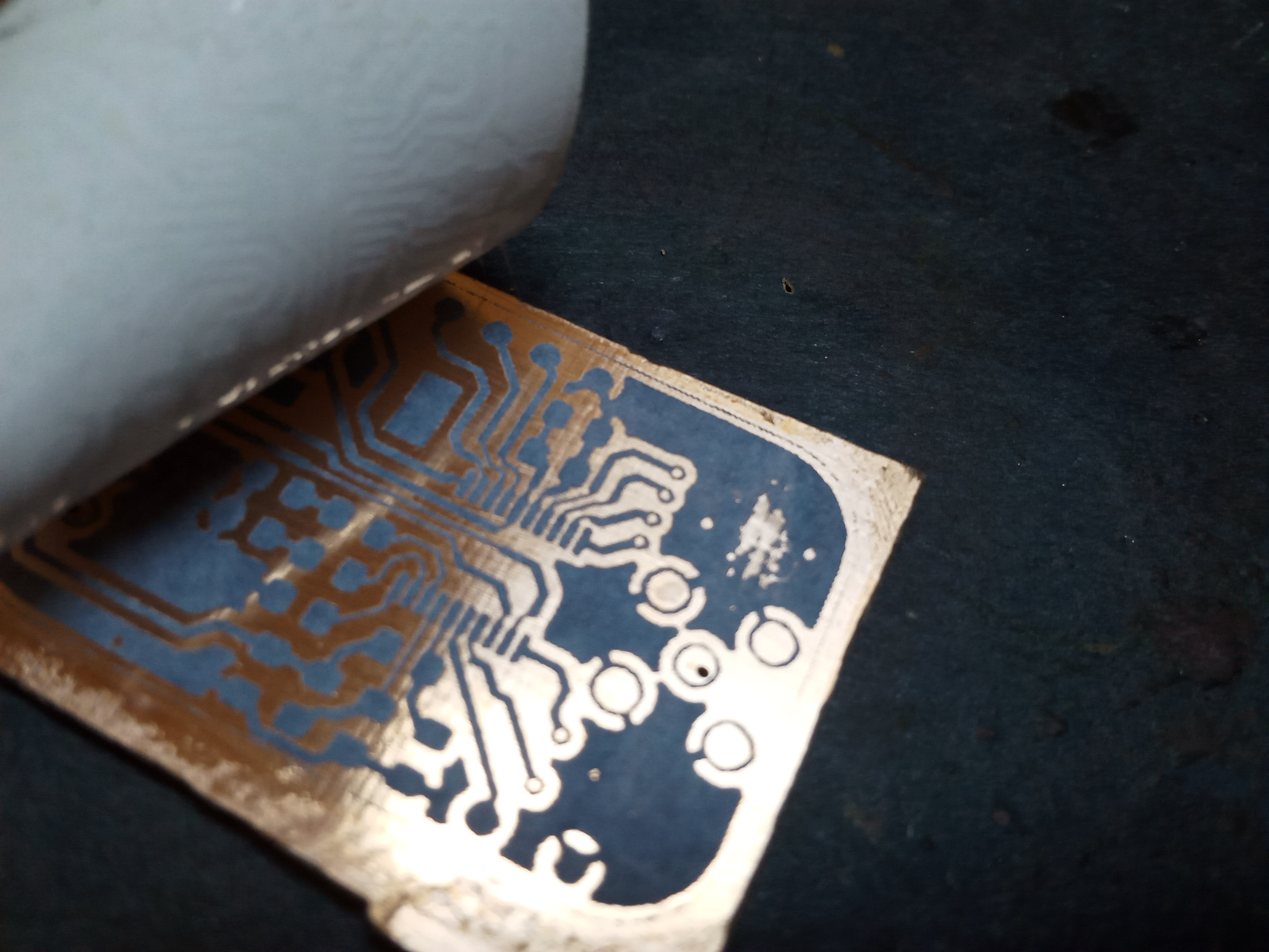
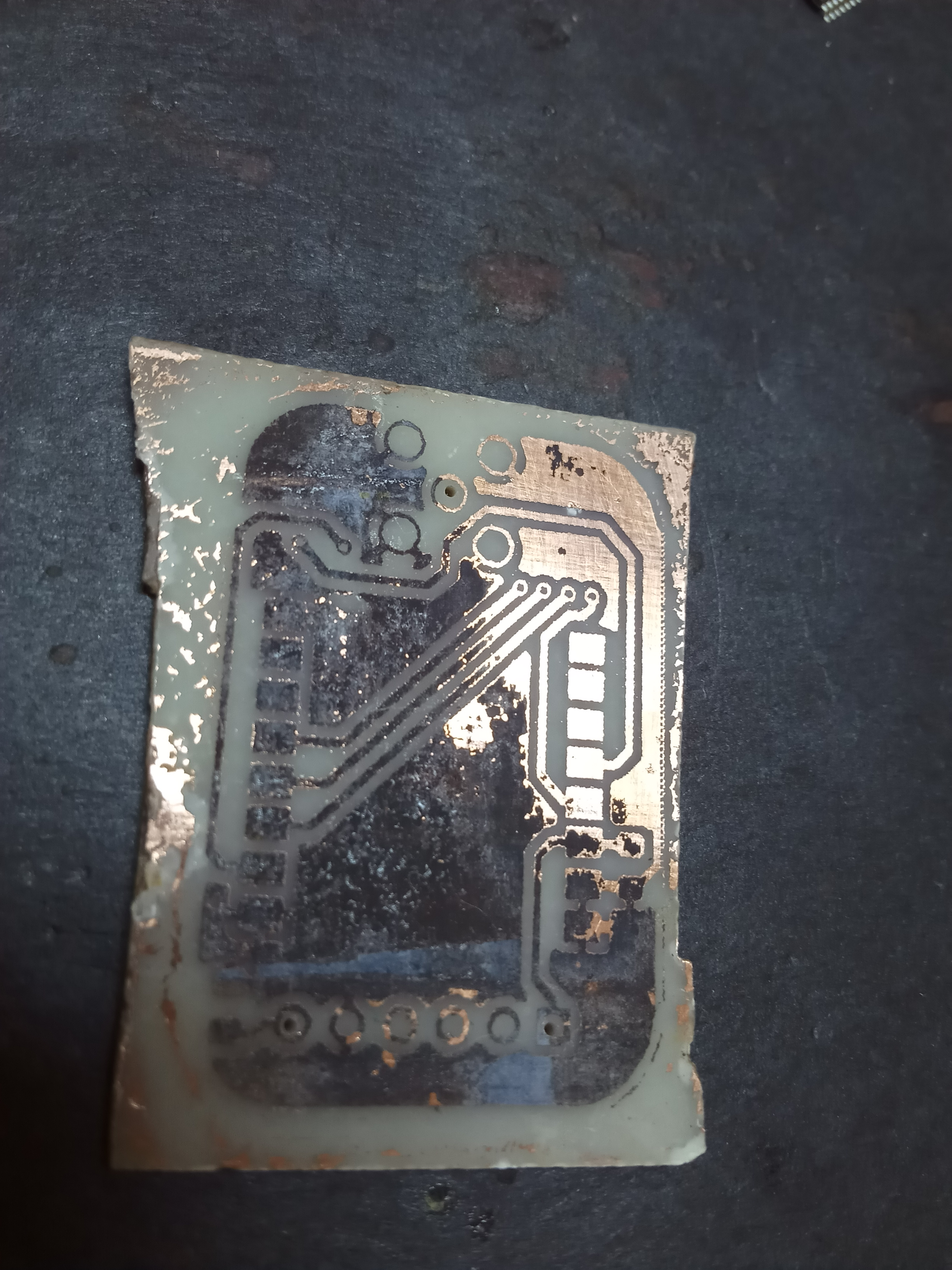
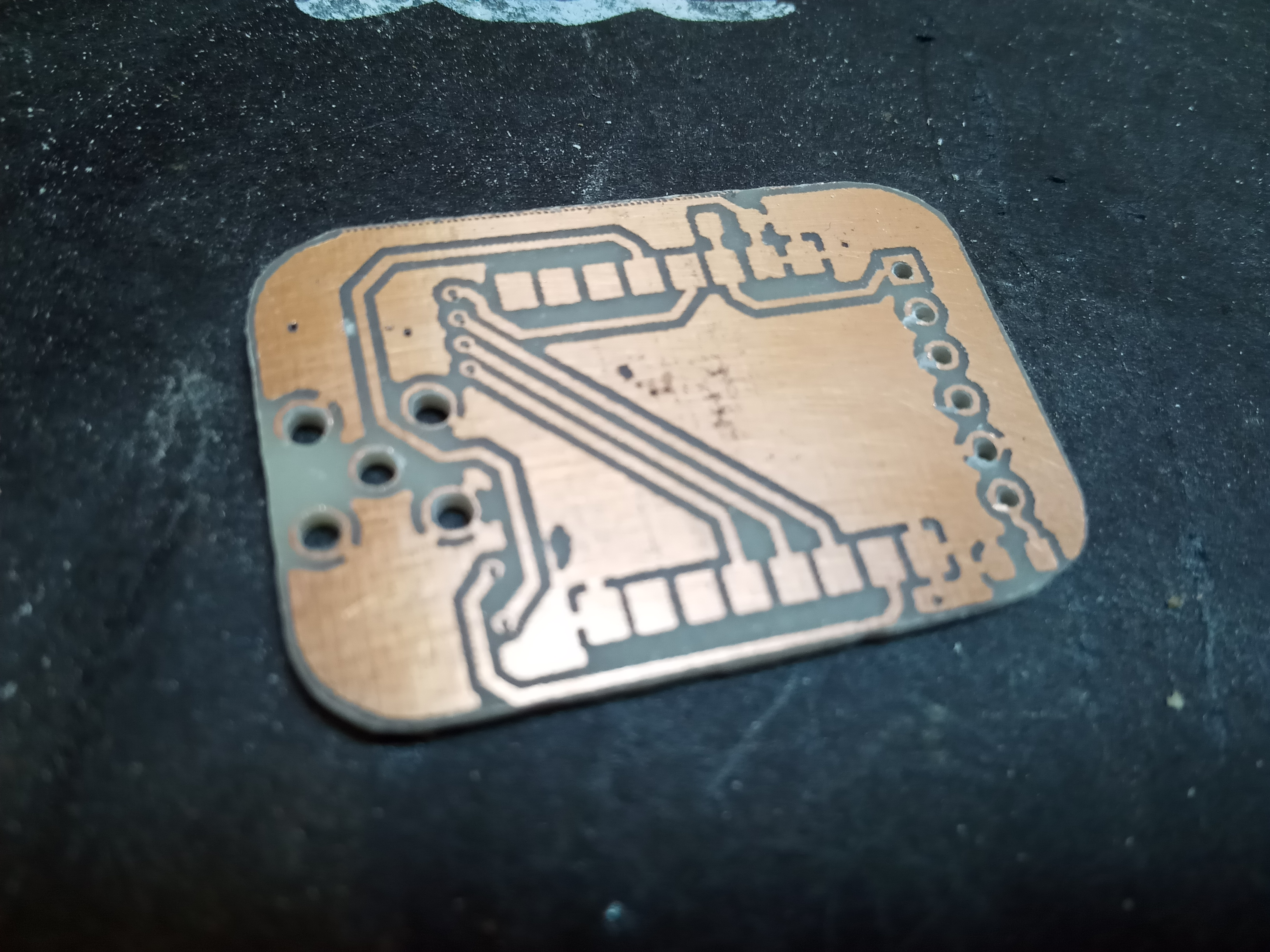
Try to peel off the tape without taking the matte paper with it; I find it easier to peel off the paper without the tape in the way. Now, starting with one corner, very slowly and gently peel the matte paper off the board being mindful not to chip toner off the board if you have to use your nails for a start. Do not worry if there are parts of the print that did not transfer, you can always repair them with permanent marker.
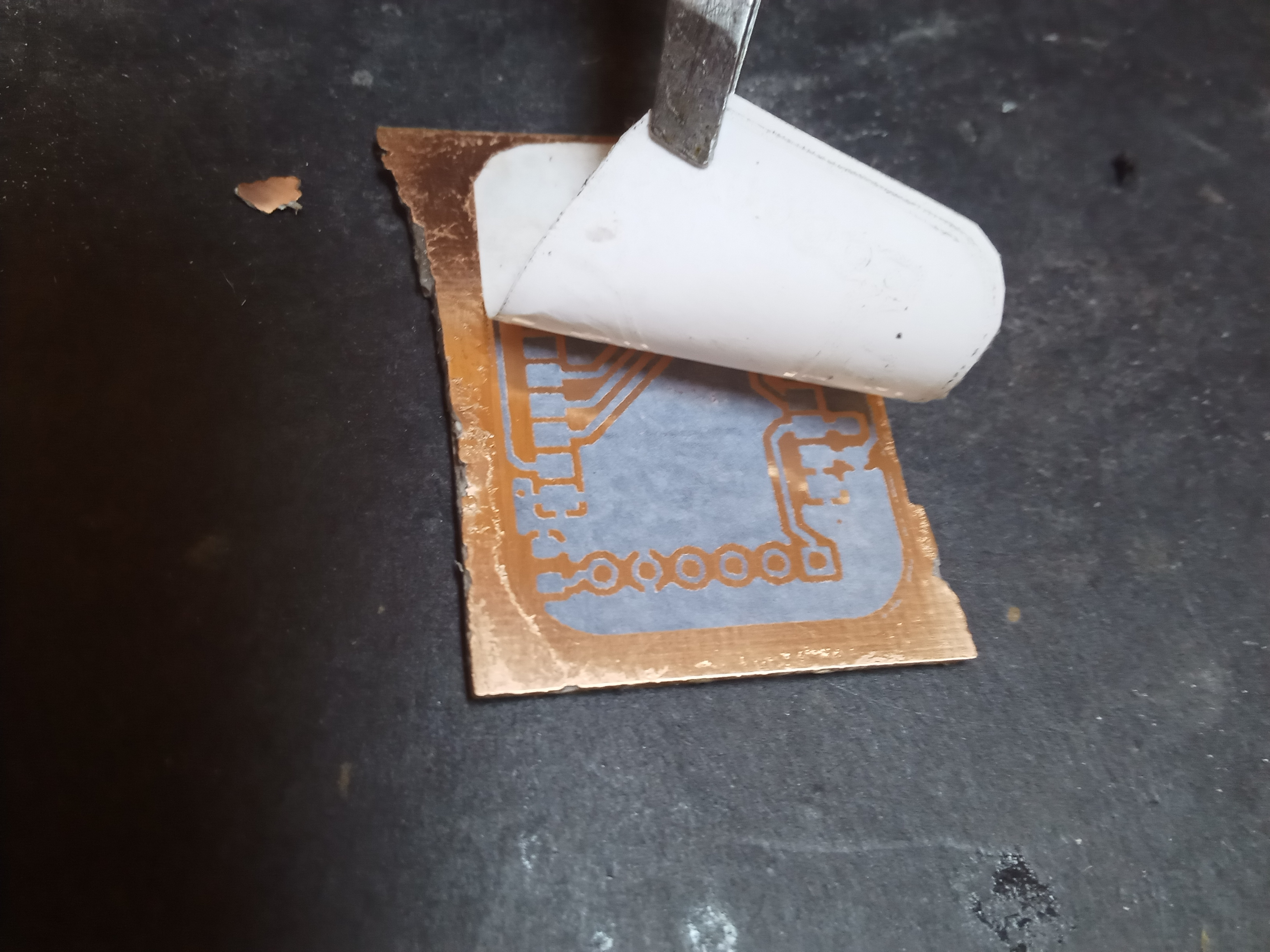
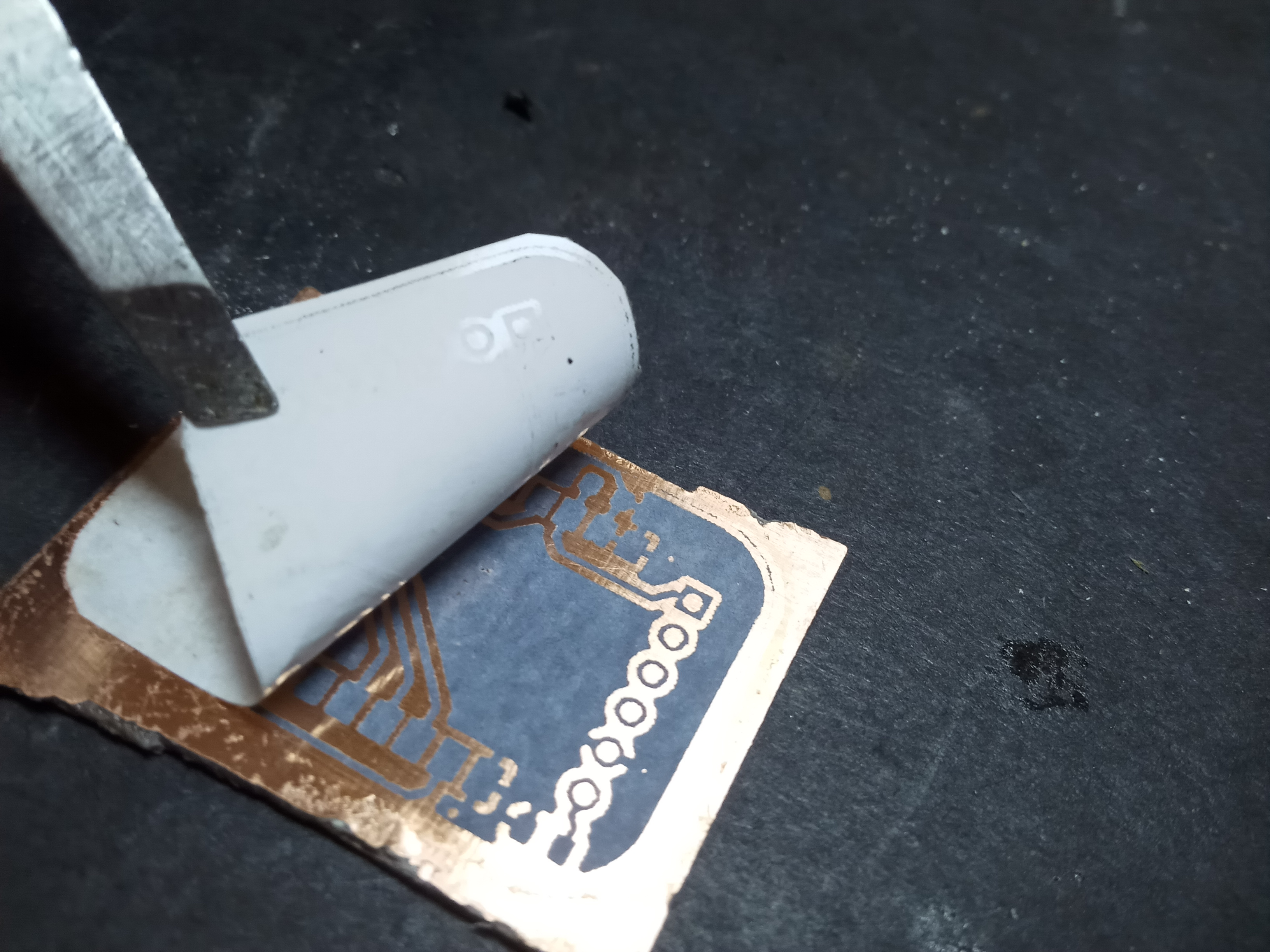
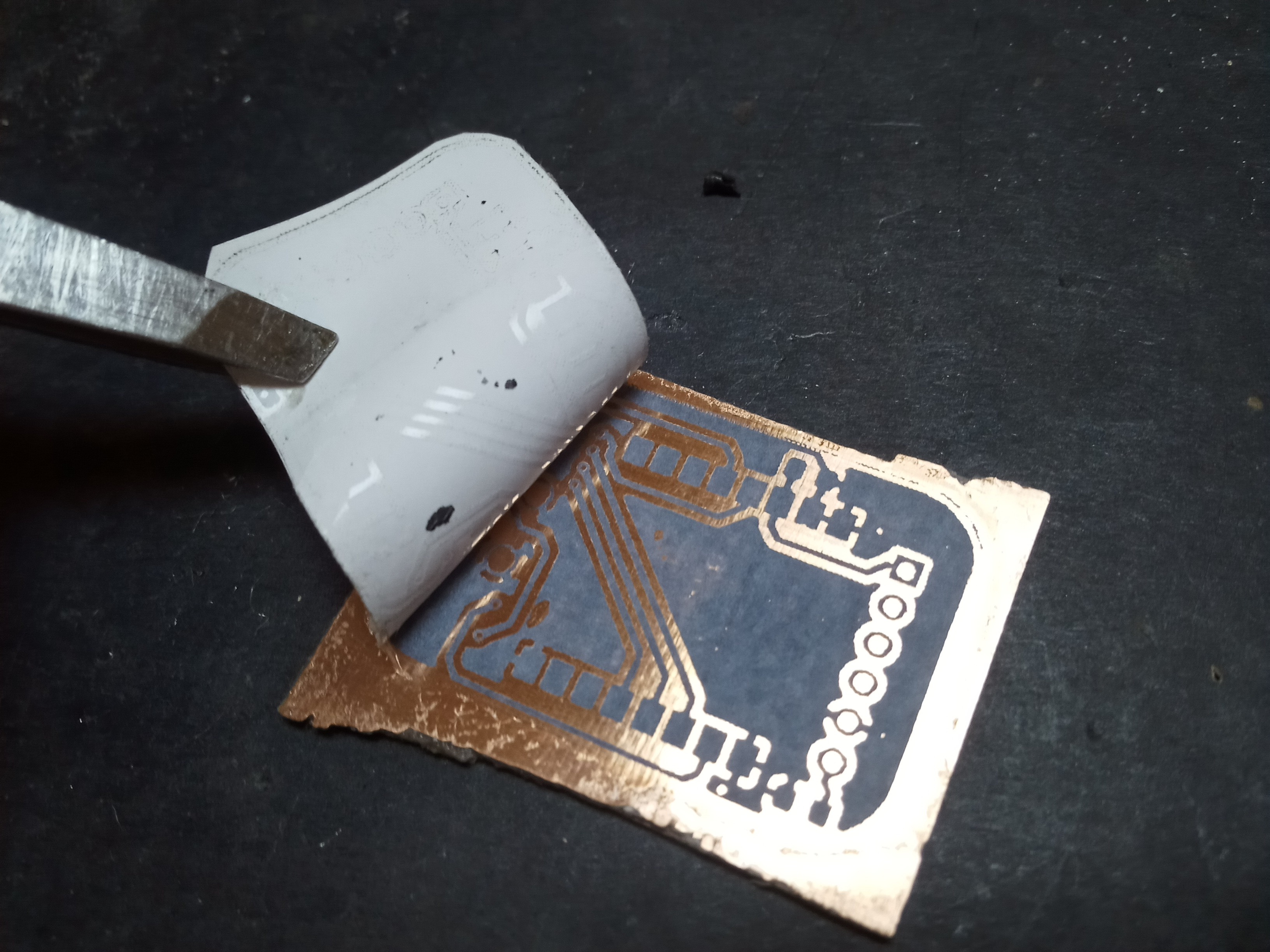
Etching the Top Layer
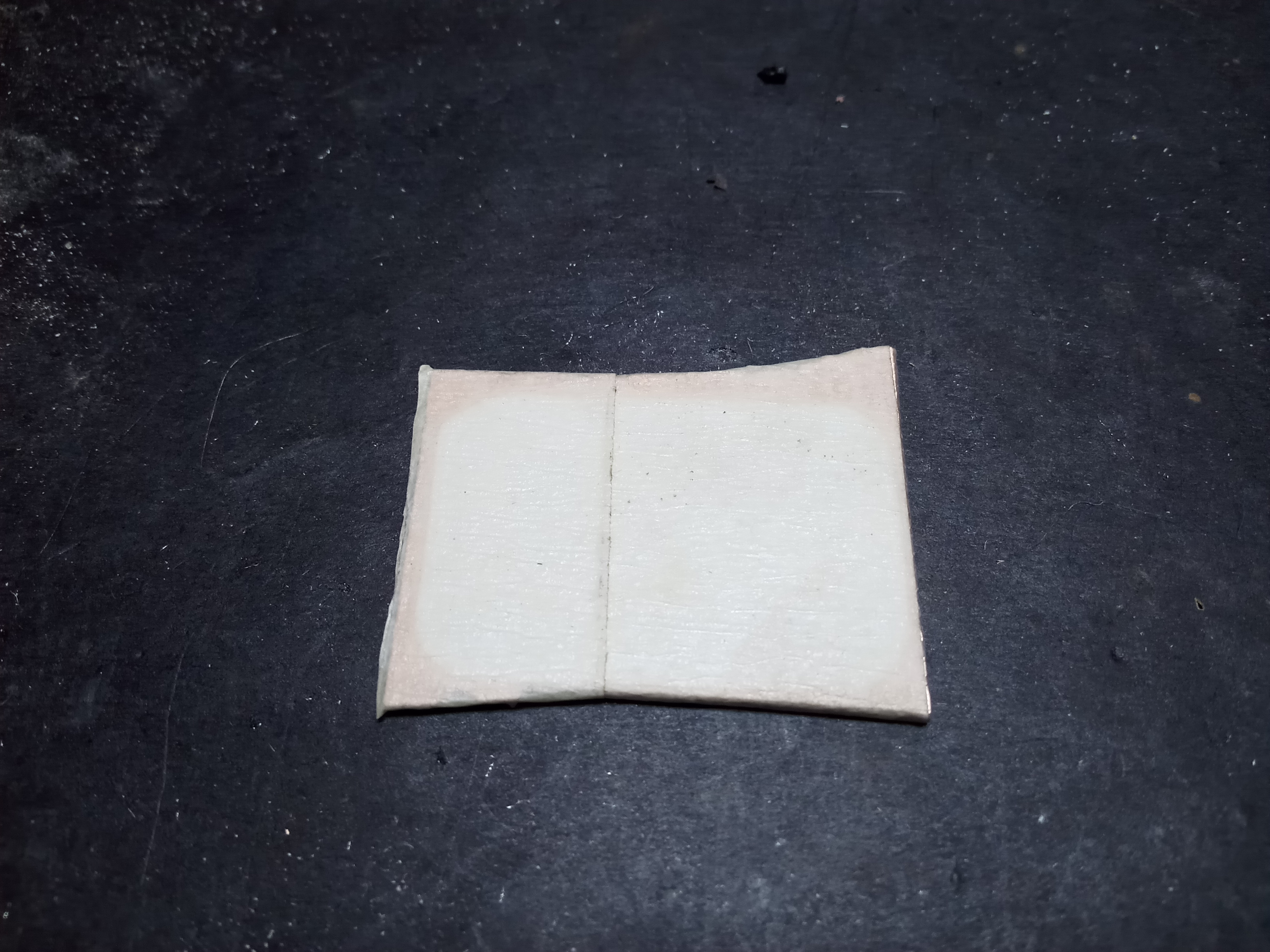
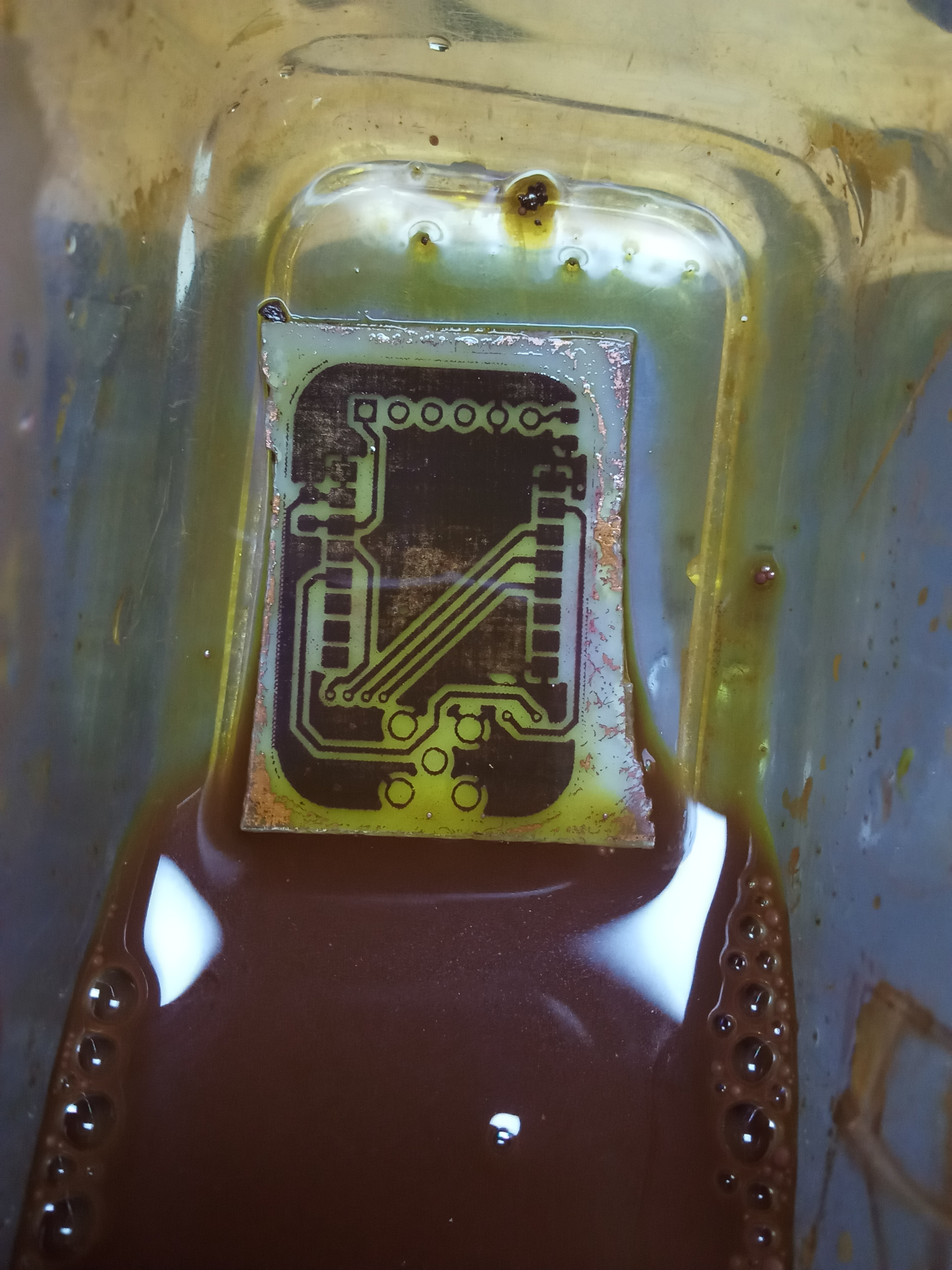
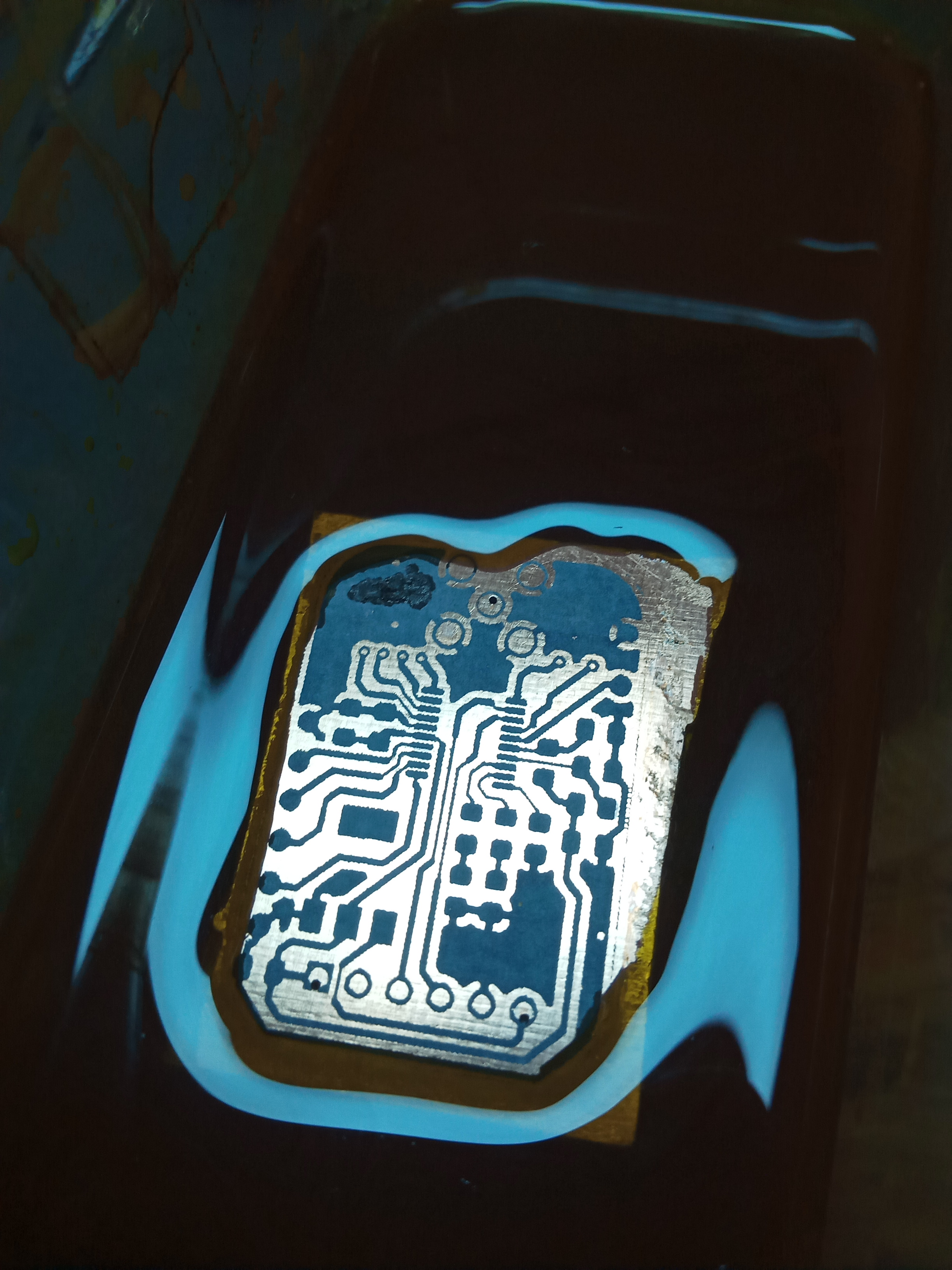
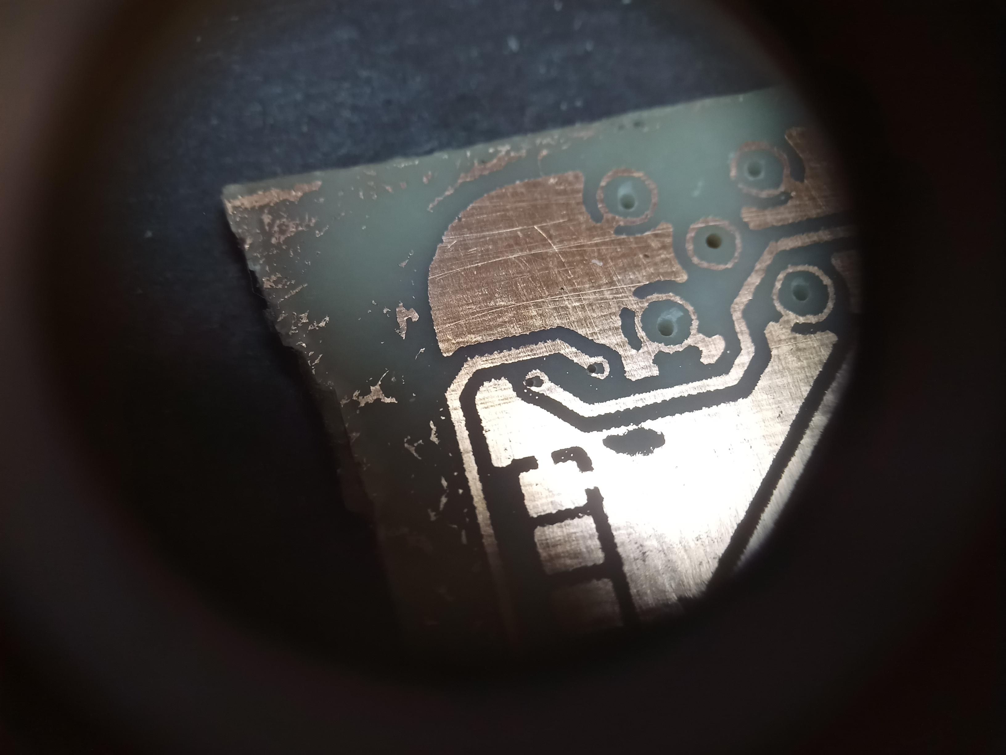
Having tried various variations of the steps when etching double-sided board, I found the best one is to transfer and the etch on one side of the copper completely before moving on to the next as the toner will not get damaged while performing intermeiate procedures. So we protect the bottom copper with some waterproof tape before immersing the board in a Ferric Chloride solution. Most of the time I just eyeball the amount of chloride to add, but a teaspoon in about 50ml of water should do the trick. A good concentration should etch your board in under a minte, so try different concentrations till you find one that works for you. Place the board in the solution, rolcking it from side to side until only the toner-coverered areas are left, then transfer it into a vat of clean water to stop the reaction.There may be some enetched copper near the edges of the board due to glue that remained behind from the tape. We shall take care of that in due course.
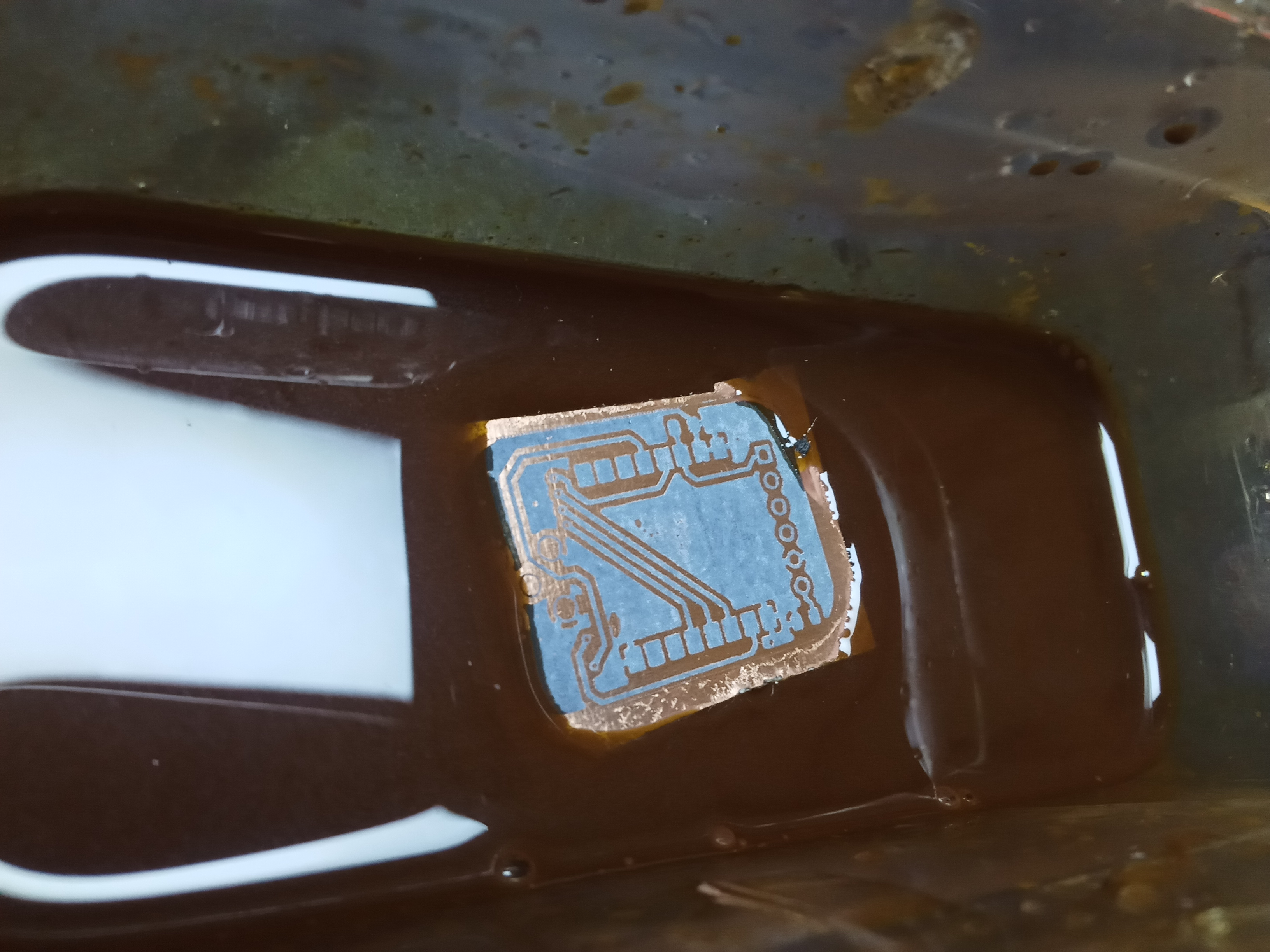
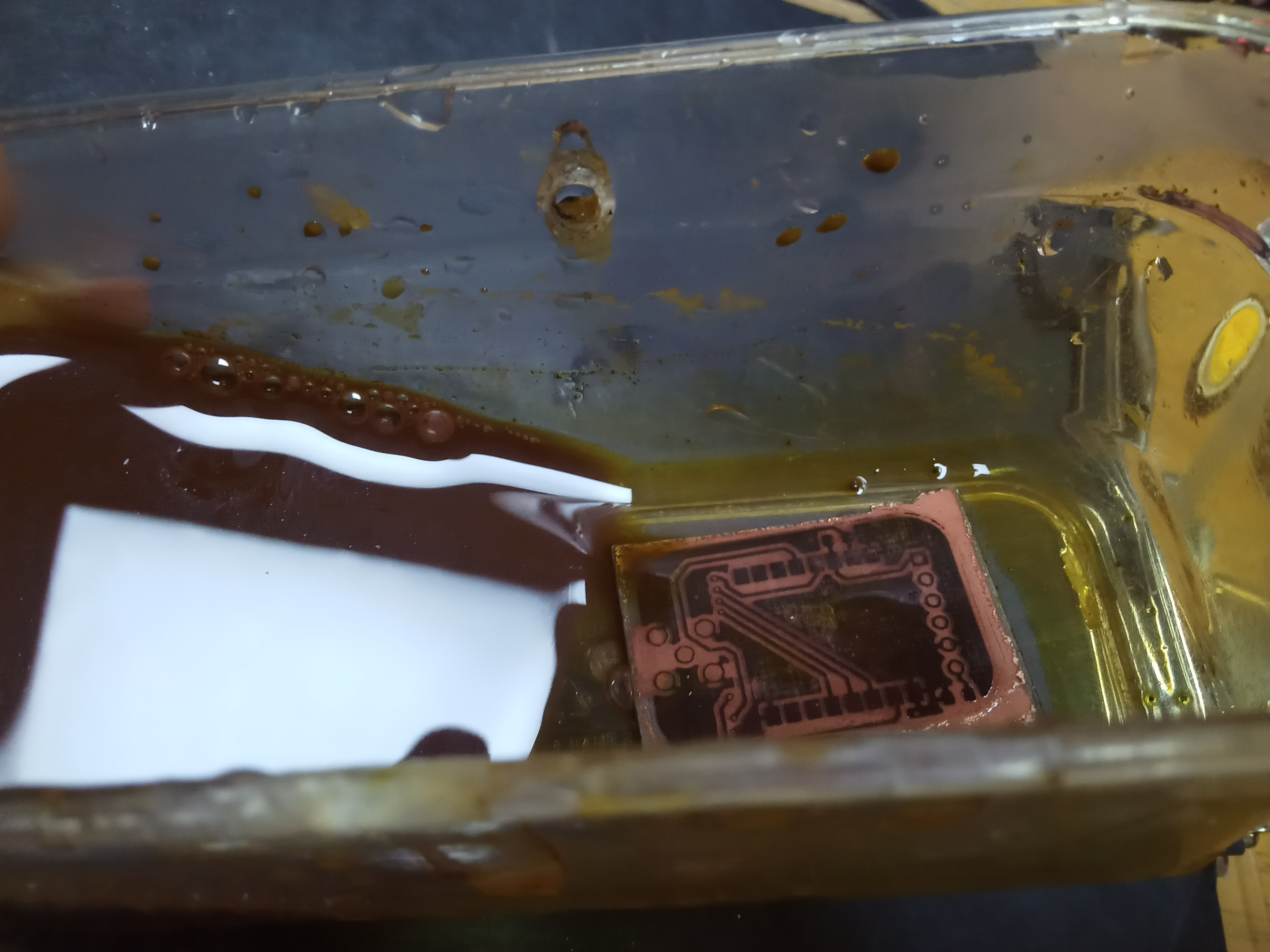
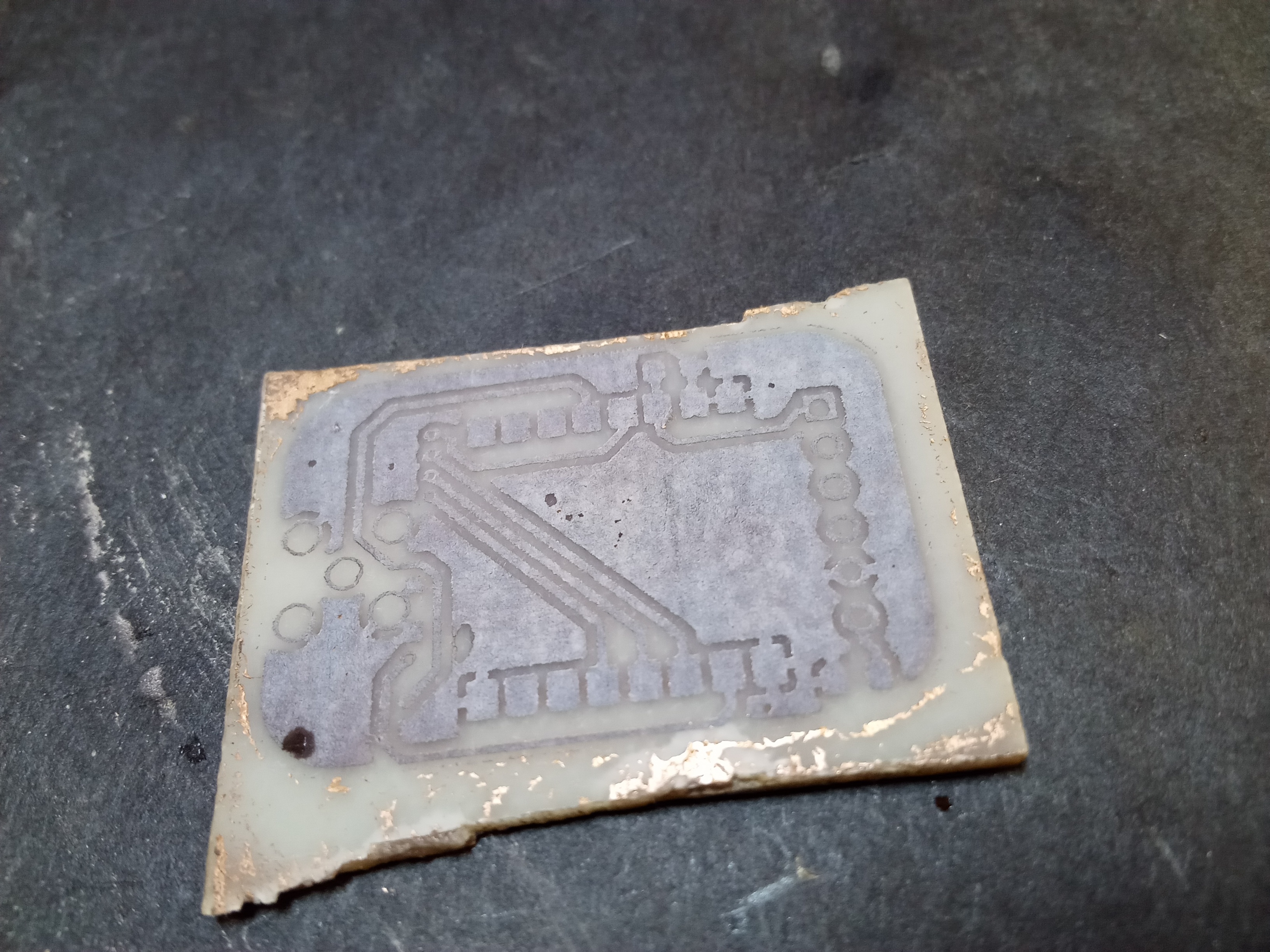
The bottom side will survive unetched through the process thanks to the waterproof shielding.
Safery Warning:
- Ensure you conduct etching in a sufficiently ventilated space as chloride fumes are evolved when the salt hits the water.
- Use latex gloves to handle the PCB while it is in the solution.
- The chloride solution vigorously eats away at metal, so do not pour it down your sink unless your drainage system is made of all PVC. You can alternatively dispose of the solution by pouring it on the ground away from any drainage or underground piping.
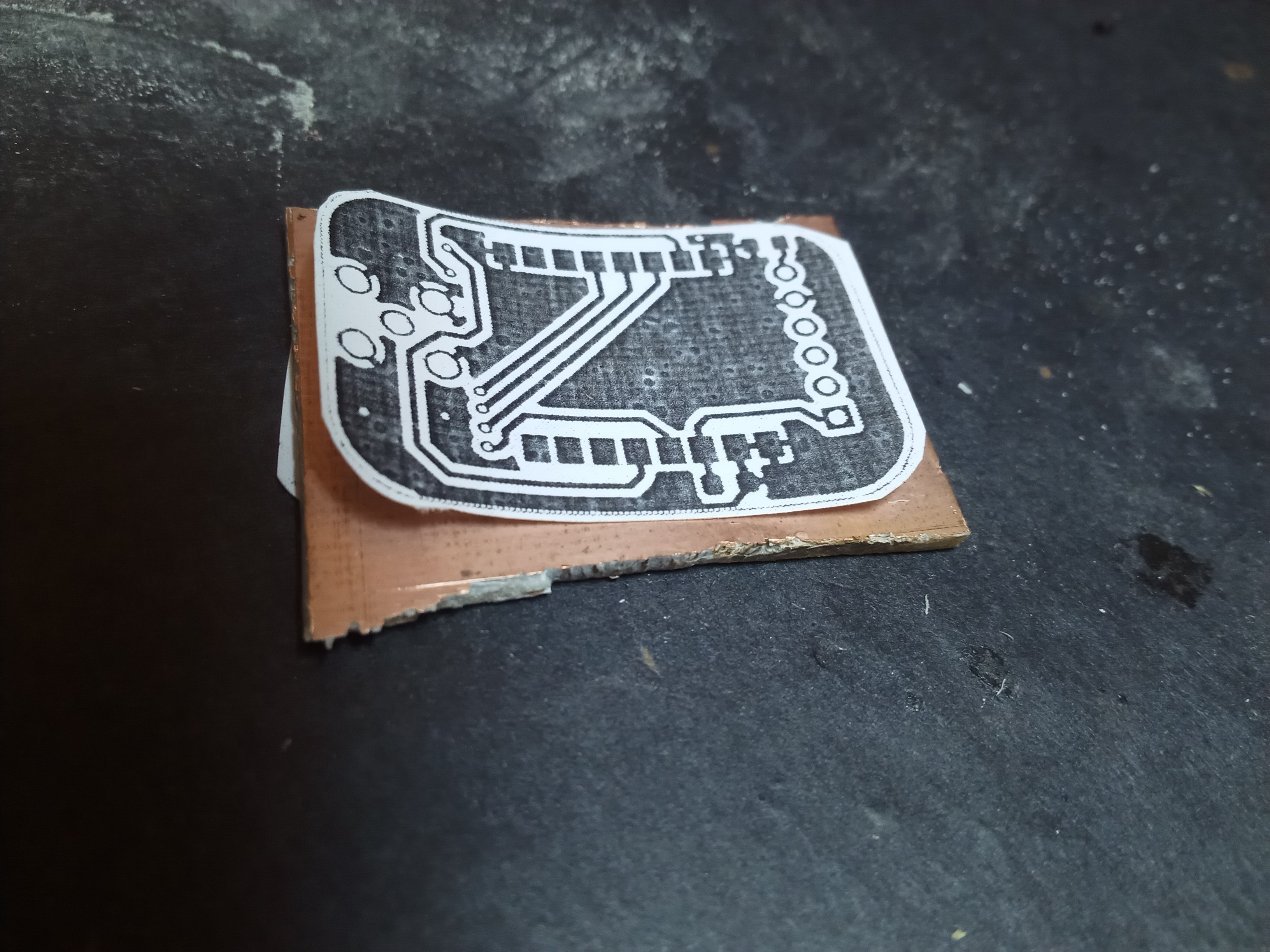
Alignment of Top and Bottom Layers
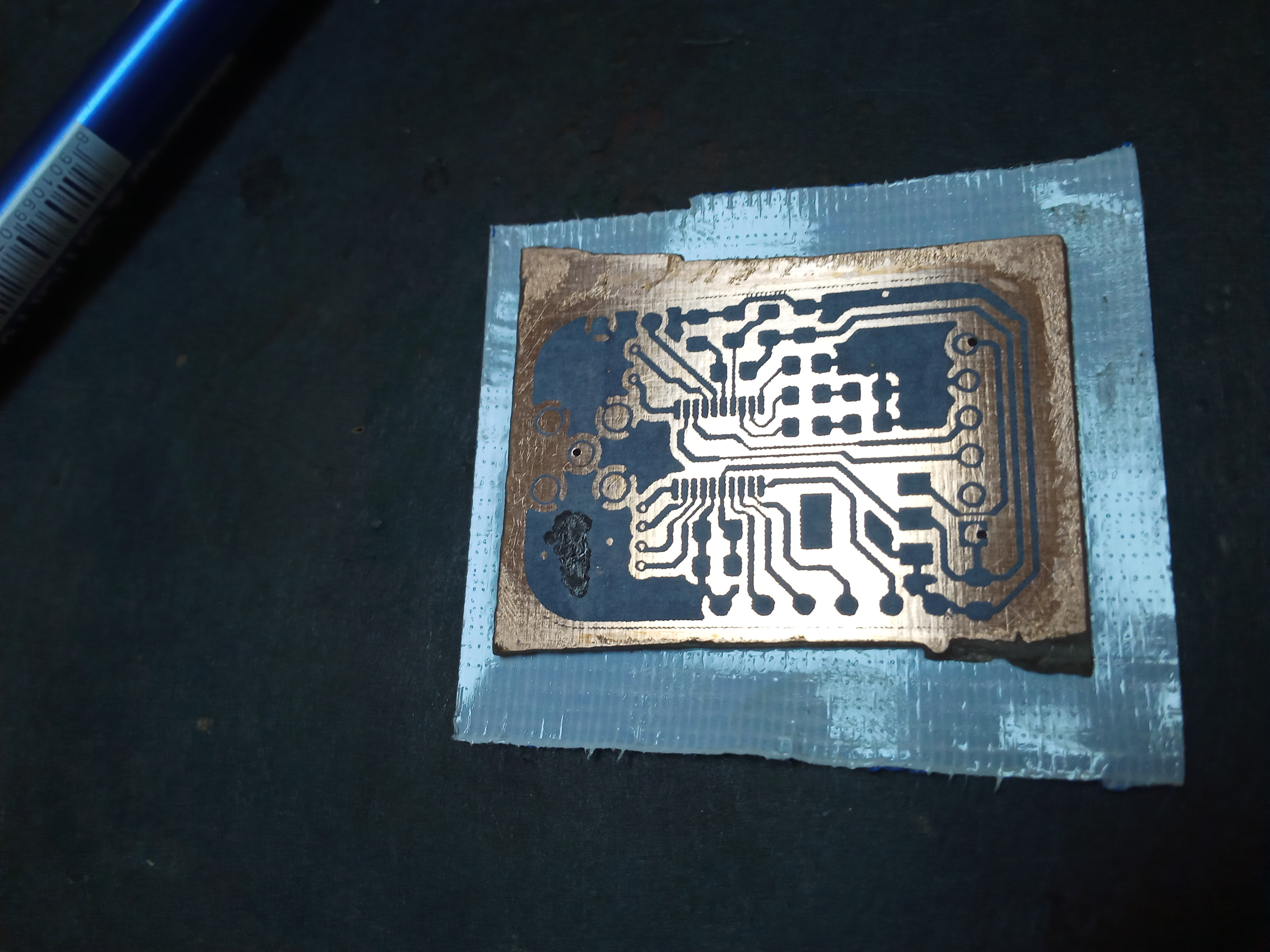
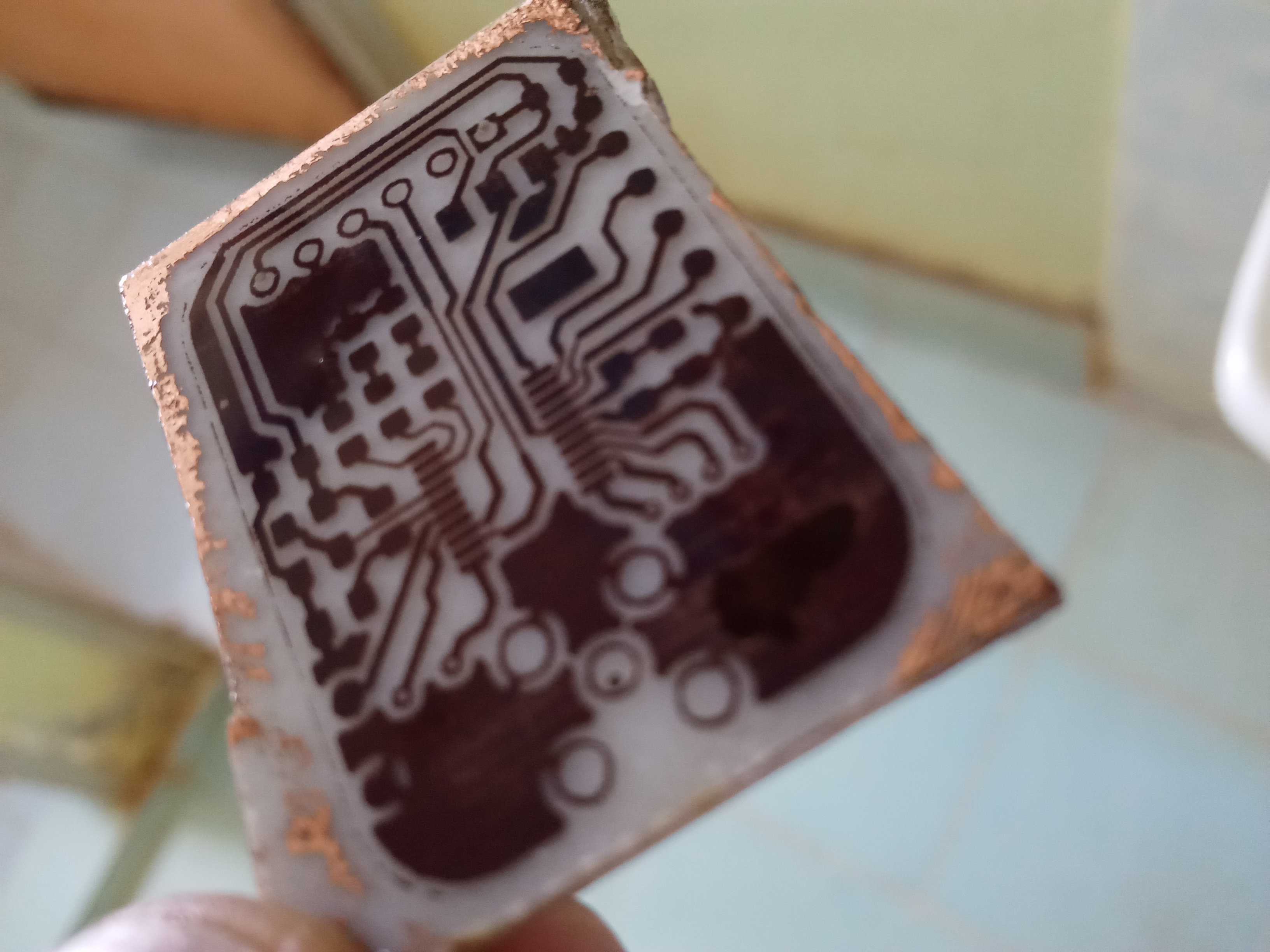
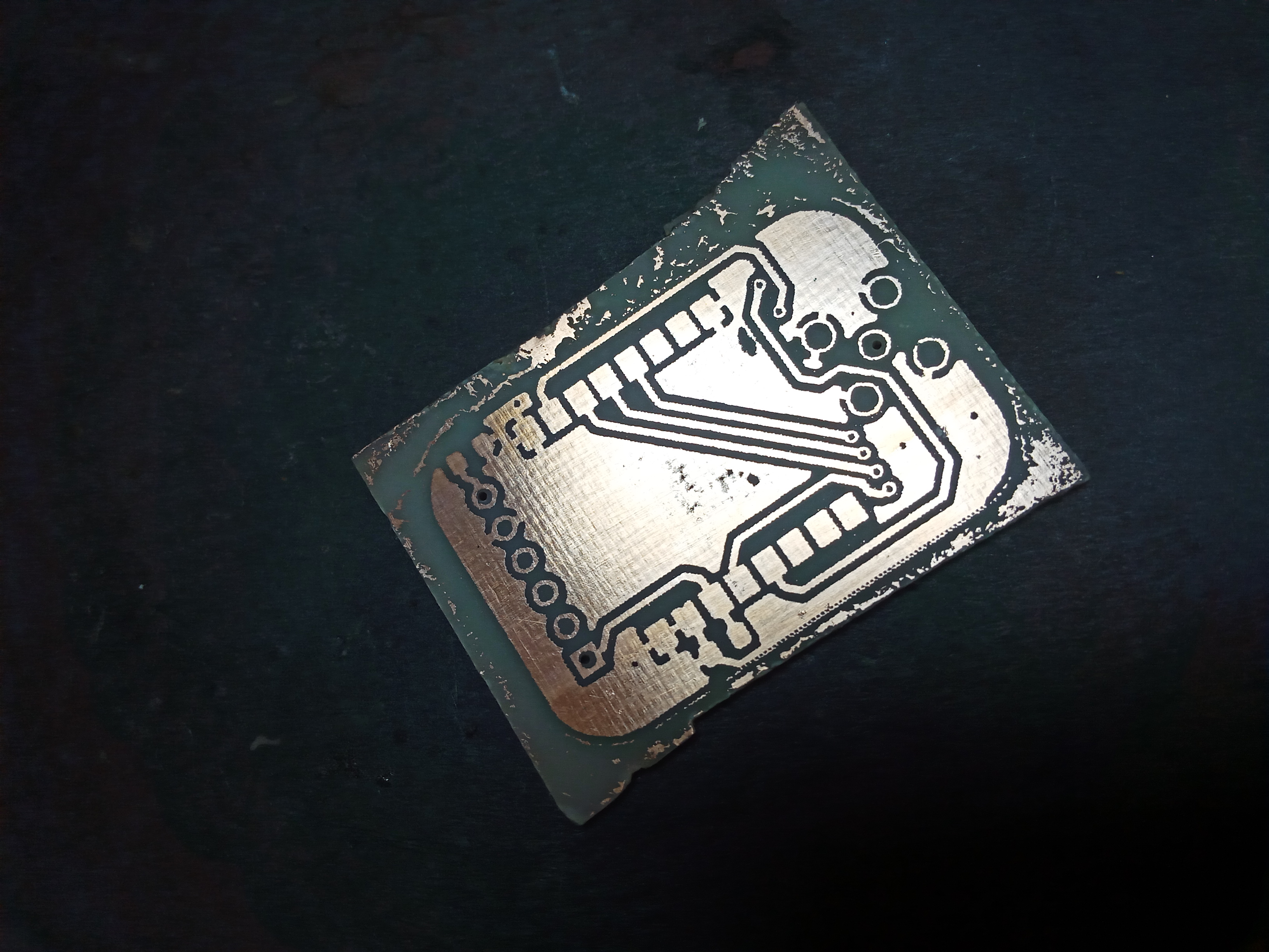
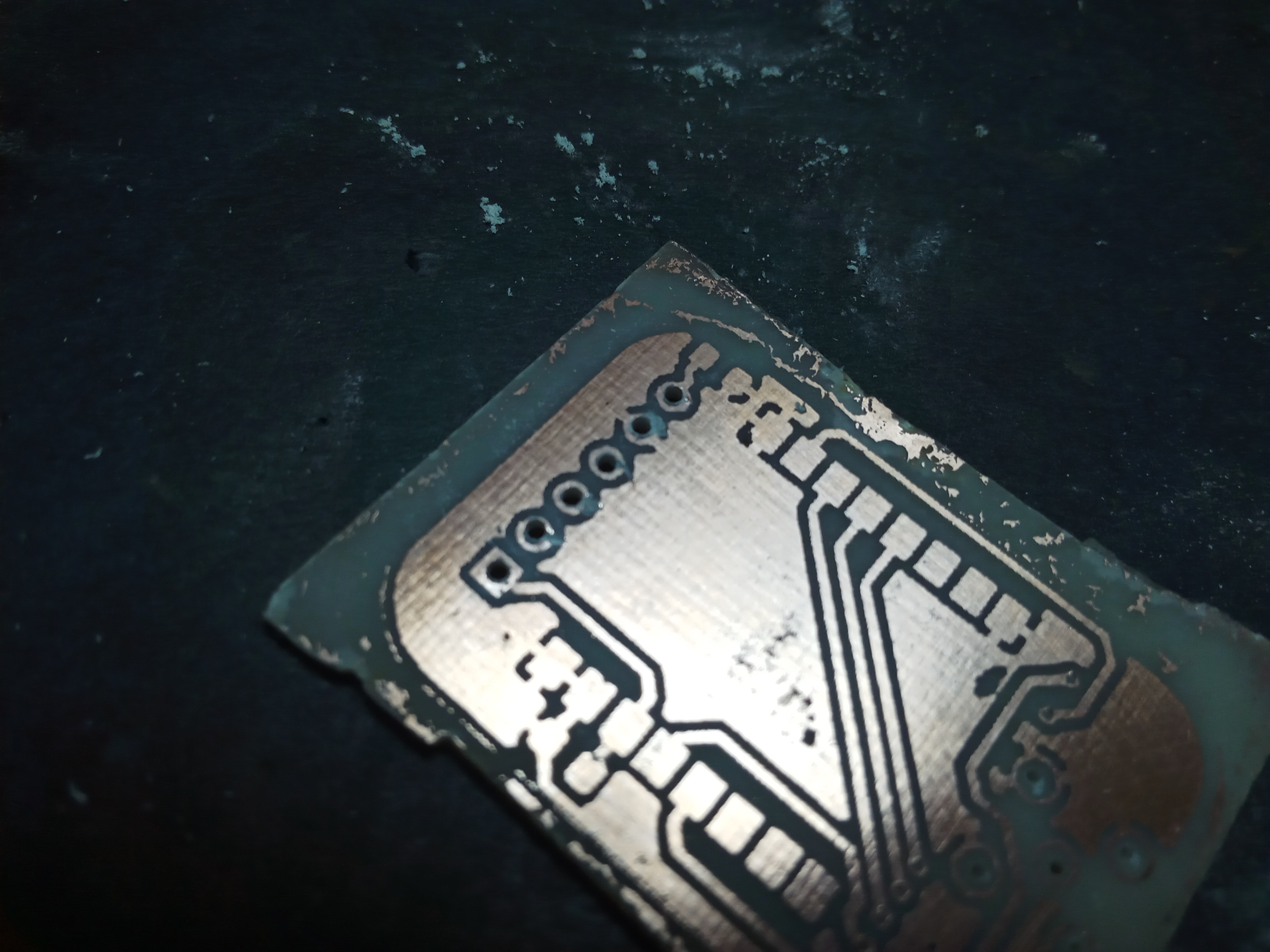
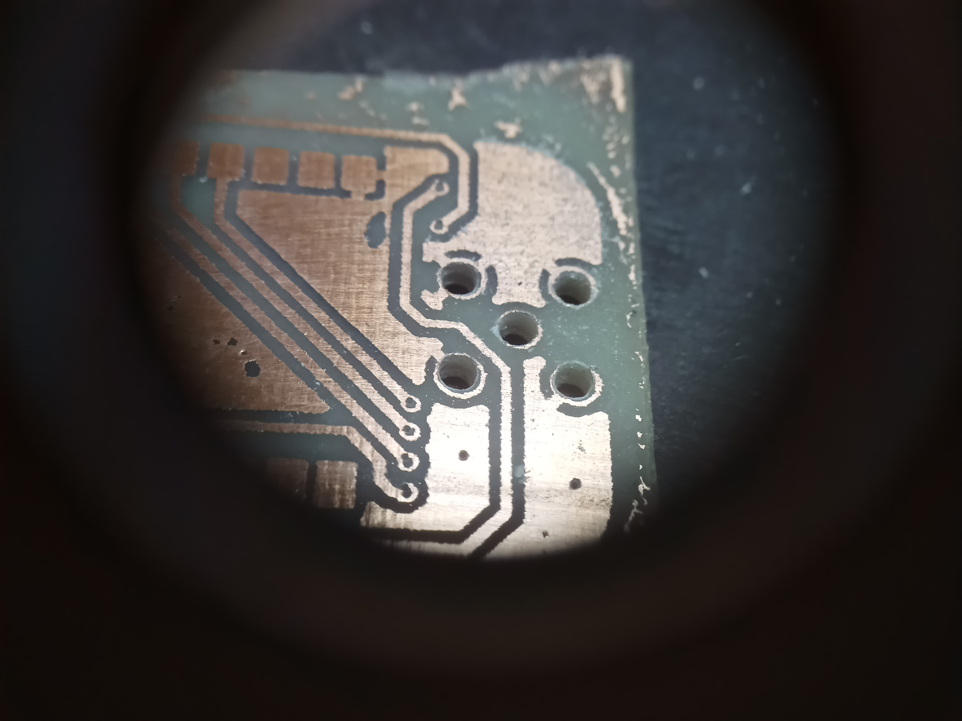
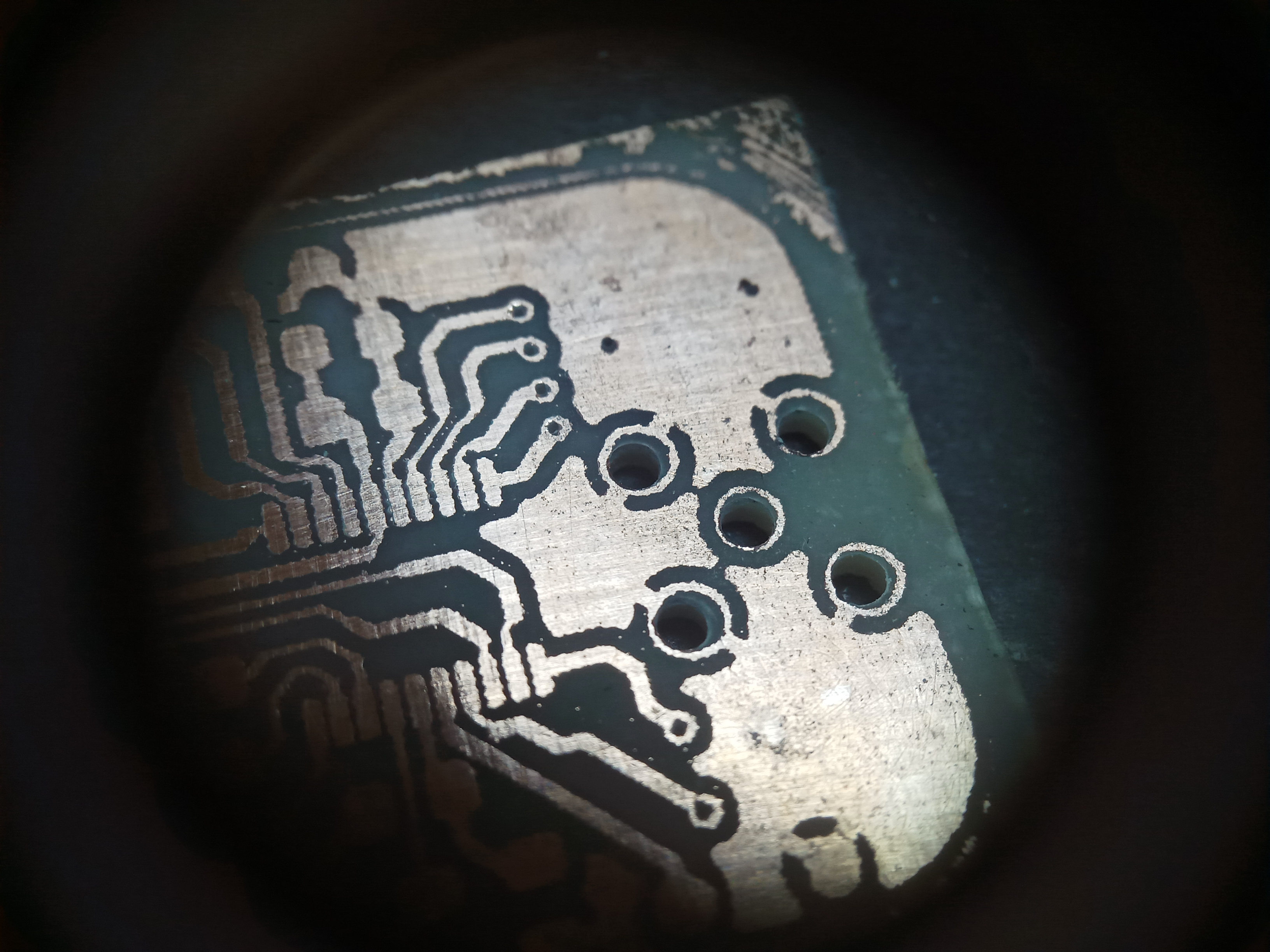
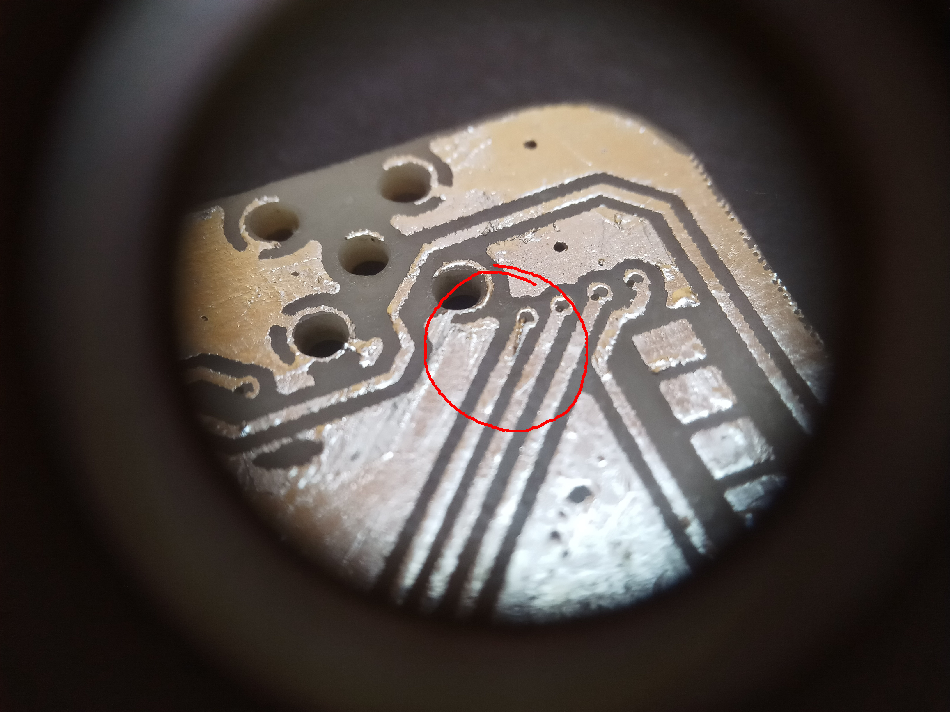
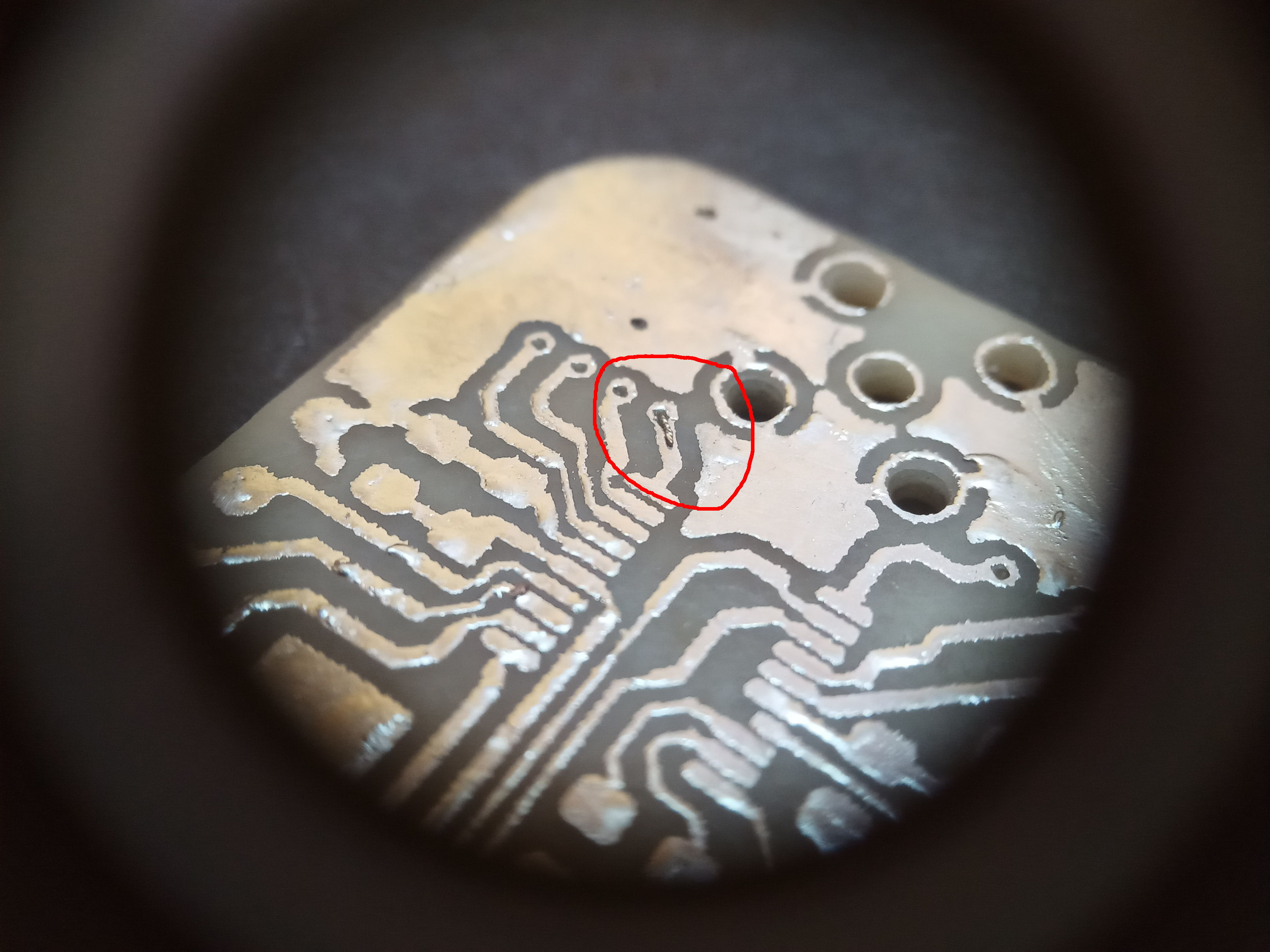
Before etching the bottom layer, we have to make sure that vias and holes of through-hole components line up on both sides of the board. To achive this, we make alignment holes using a 0.3mm drill that we shall use as a guide when placing the matte paper for the second layer. I take three through-holes/vias as far apart from each other as possible, to form as big a triangle as possible on the board. The holes we just made have their corresponding outlines on the bottom layer matte paper; drill them out as well. Make sure to scrub this layer to a lustre before proceeding to the next step.
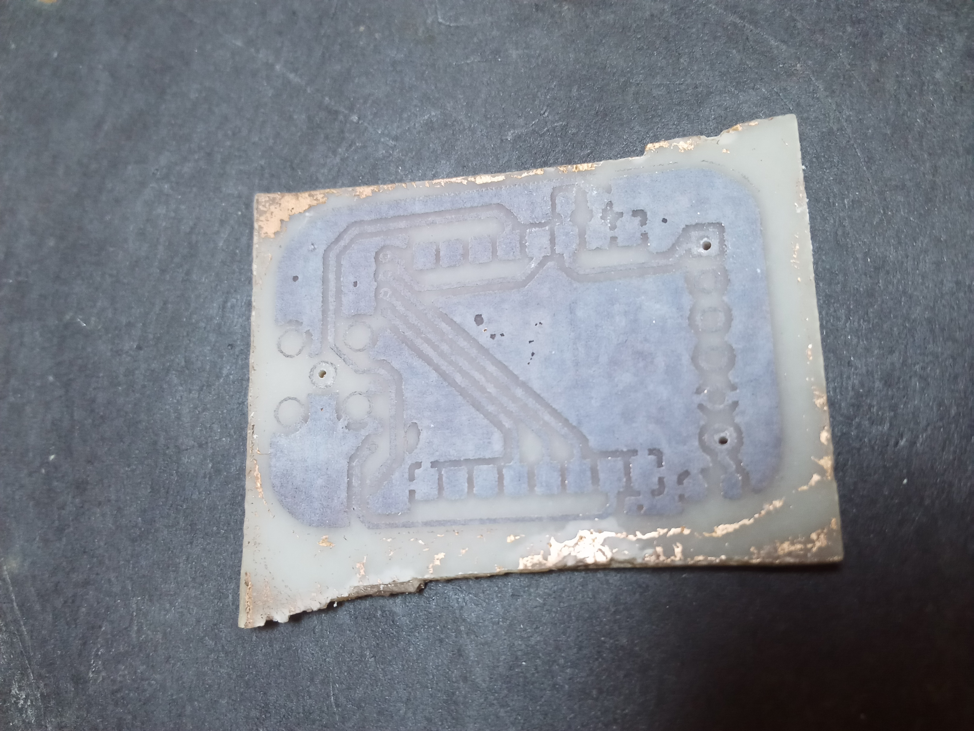
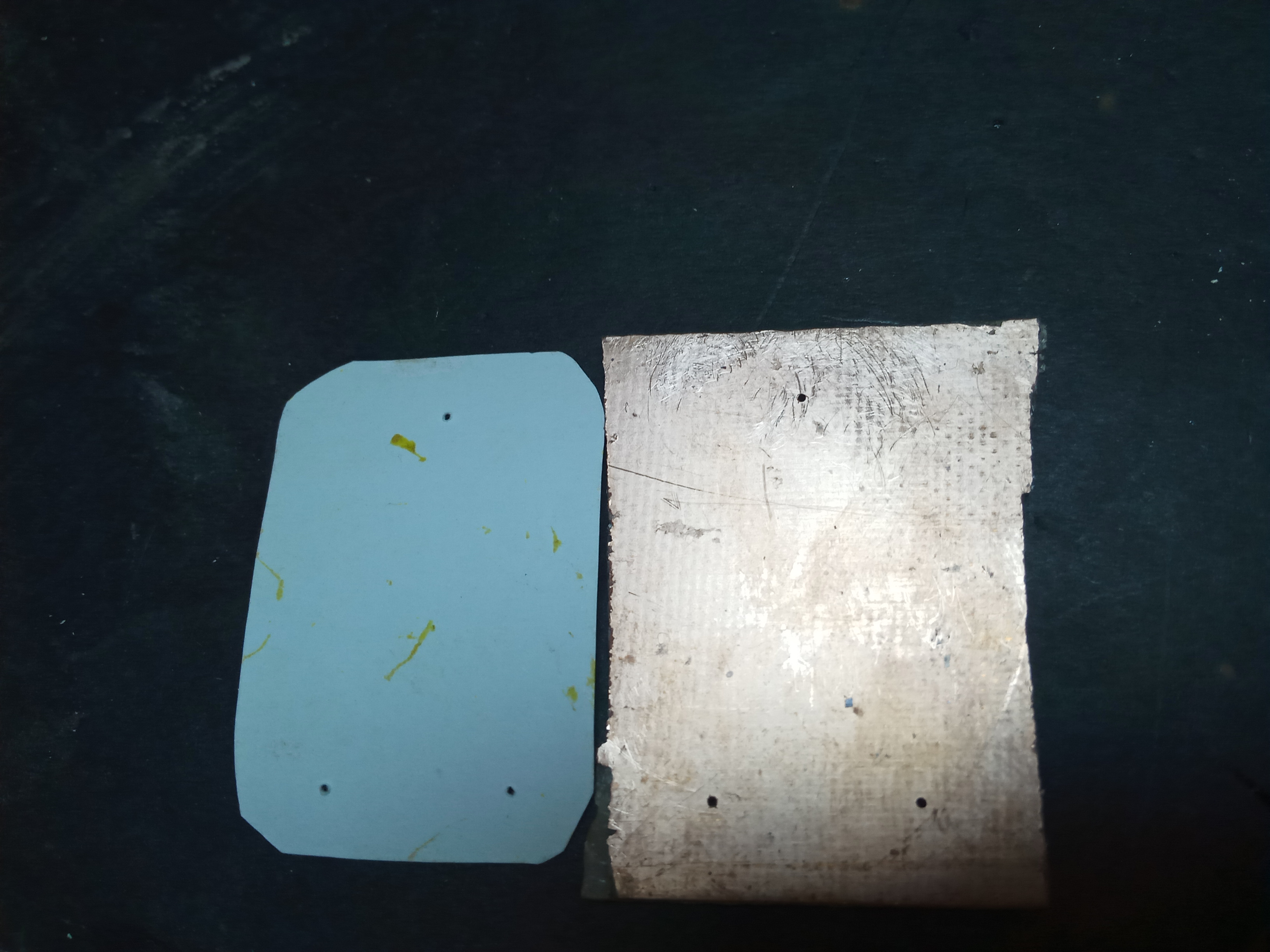
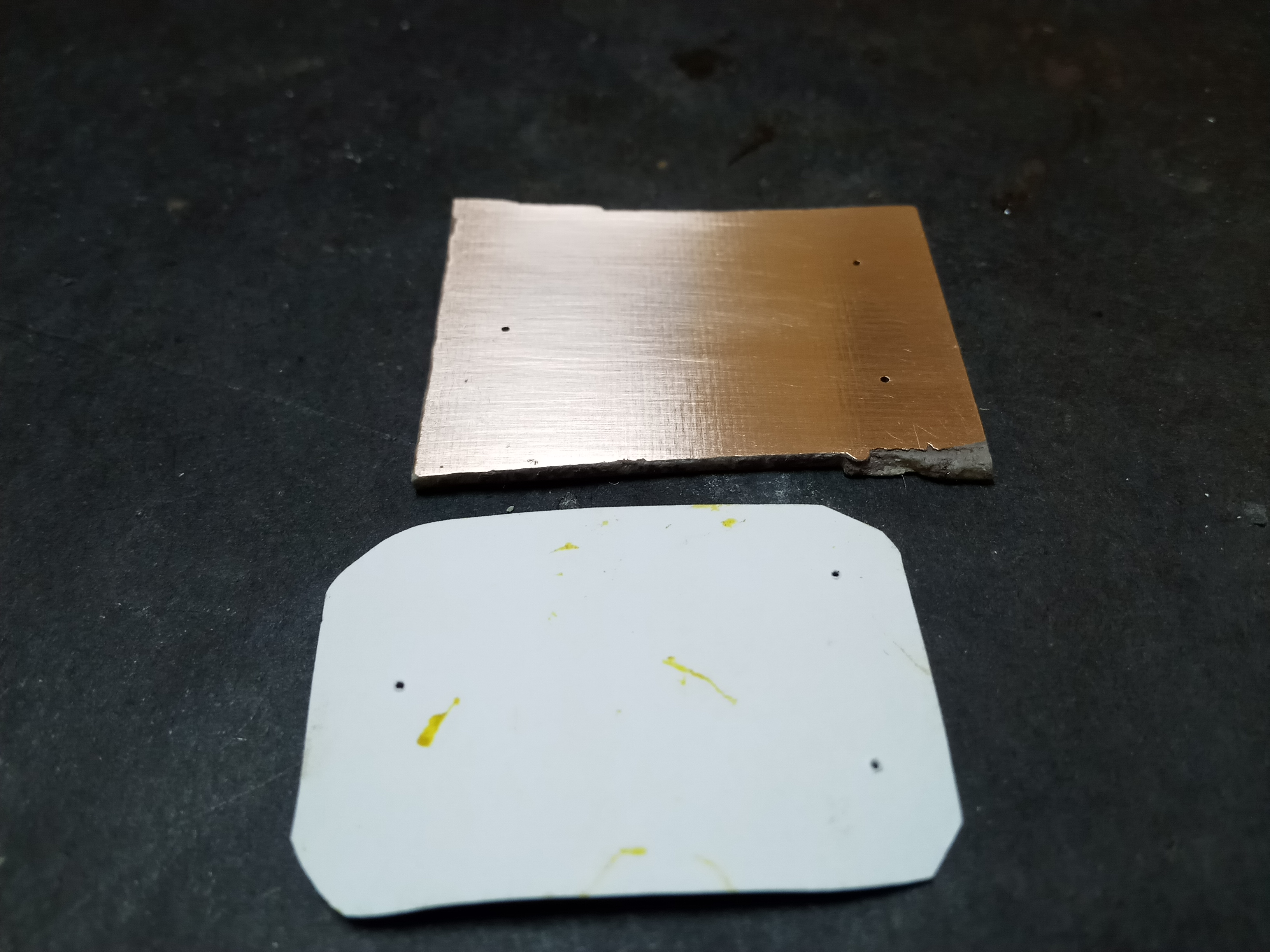
The alignment pins I am using are trimmed leads from resistors I used long ago and kept for just this kind of occasion. Needles work just as well. Place the pins in the alignment holes and the matte paper face down on the copper surface with the pins sticking through, then tape over it at the centre, making sure to keep the pins perpendicular. Having secured the paper in place with tape, remove the pins and tape over the rest of it. Iron over this layer just like the top layer then it cool down over a coffee break. We are a third of the way through the process.
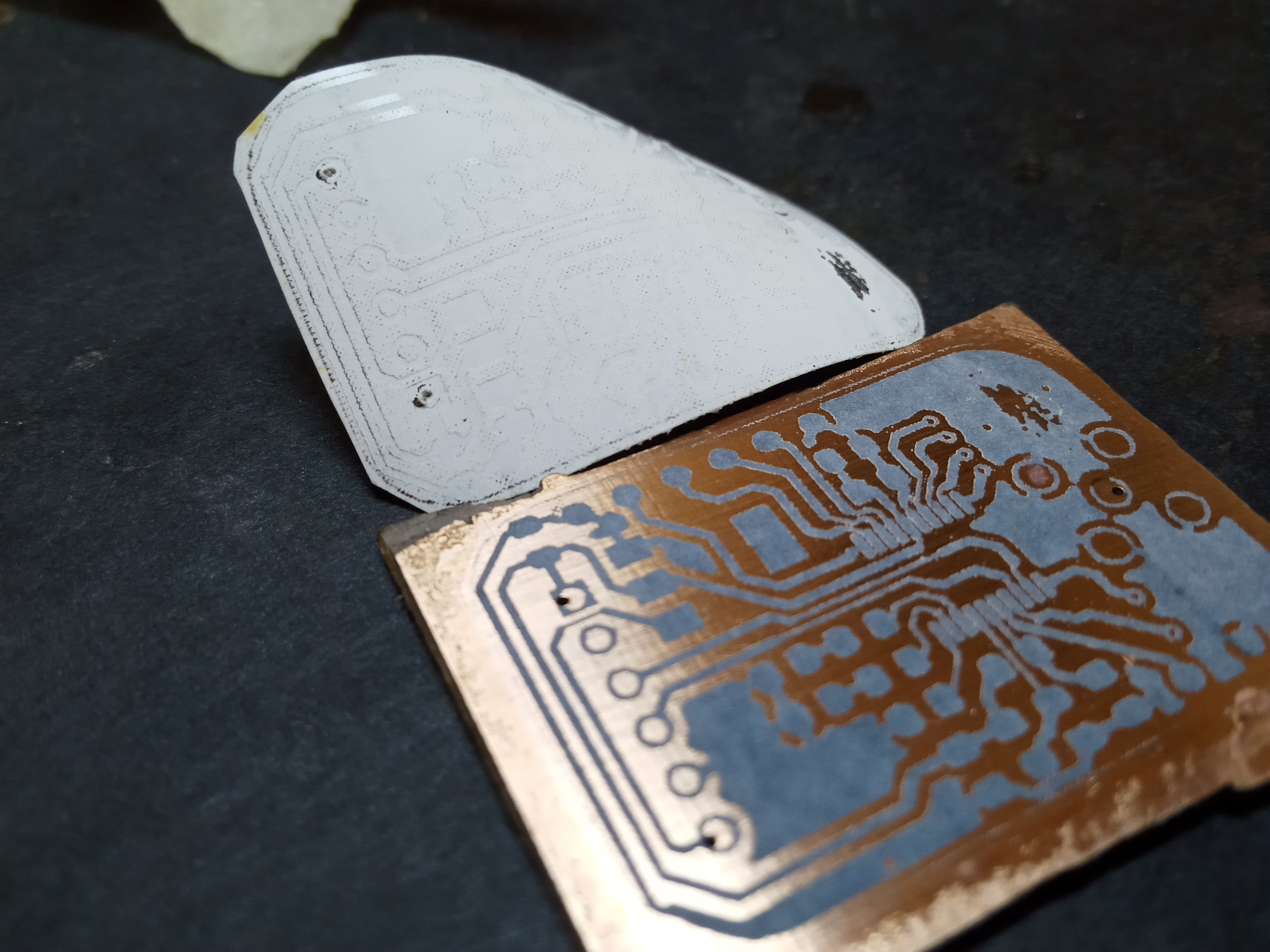
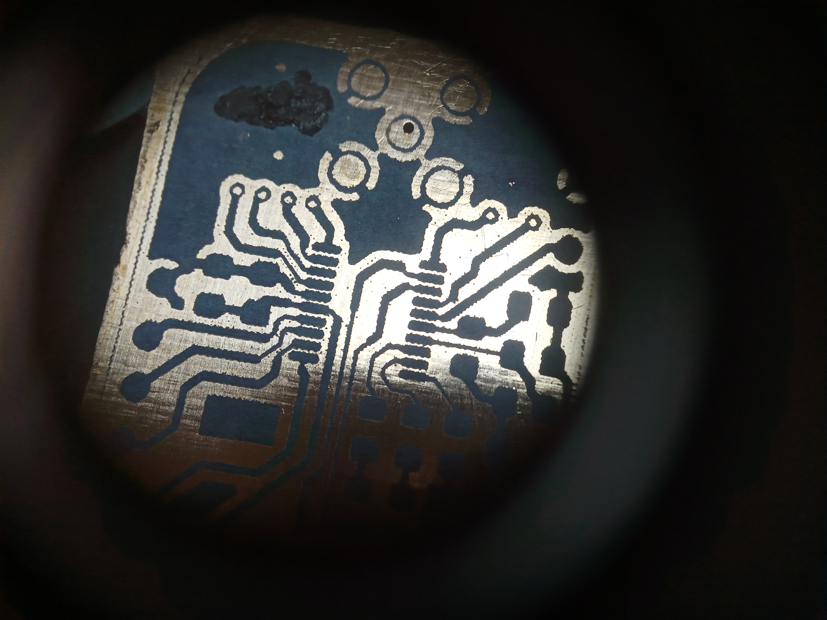
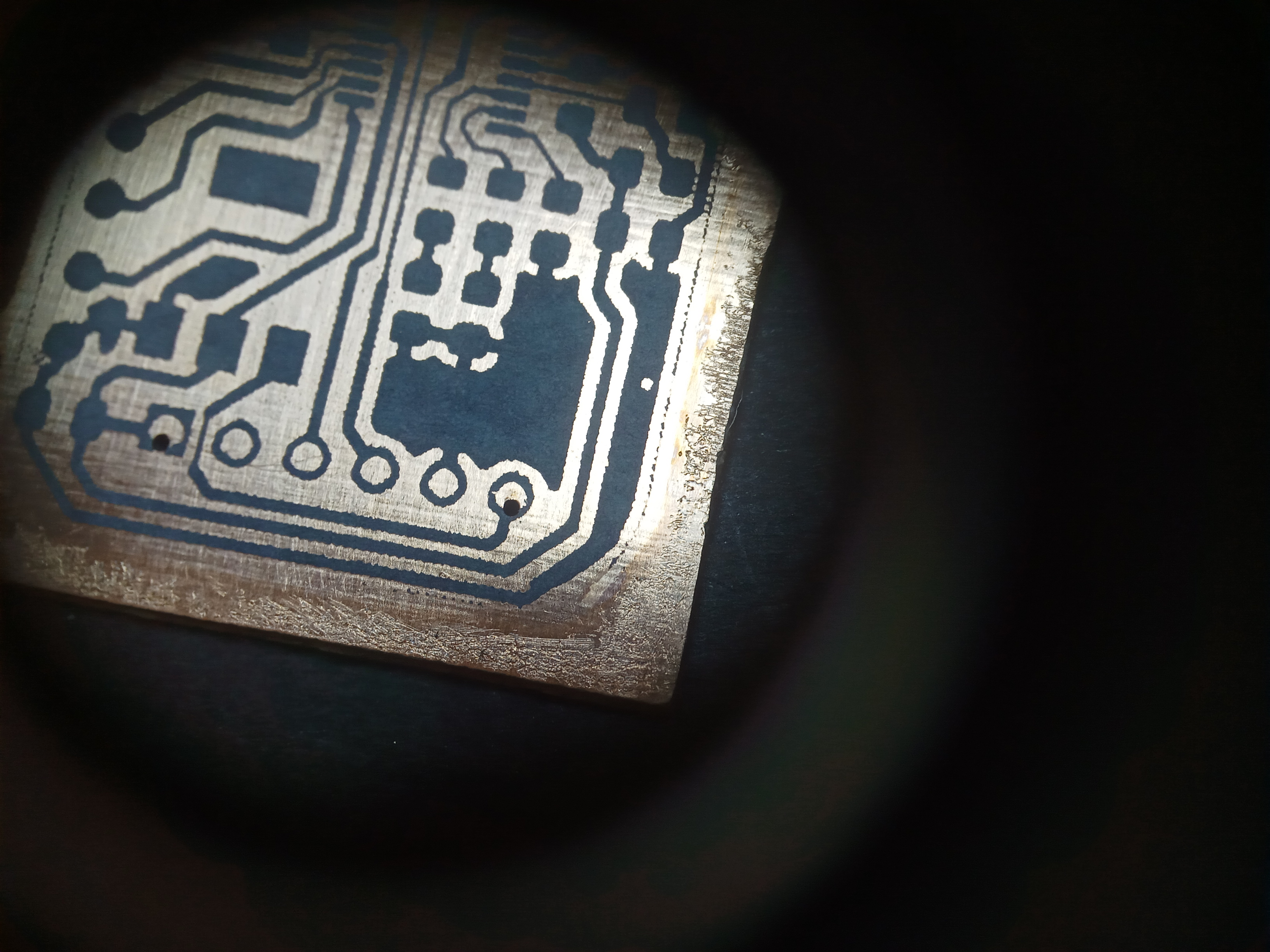
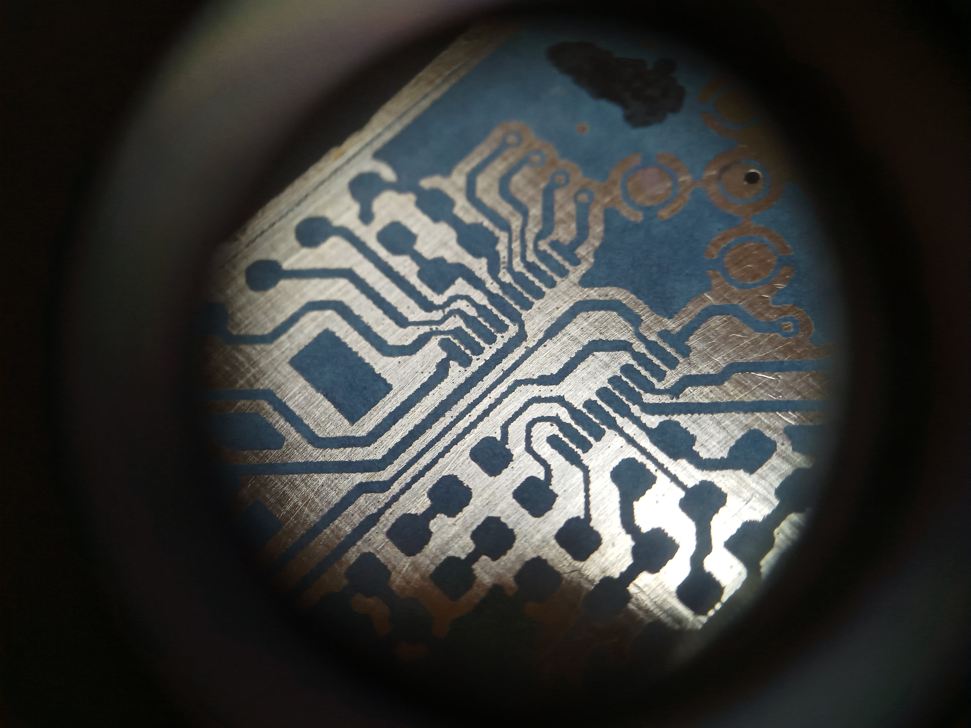
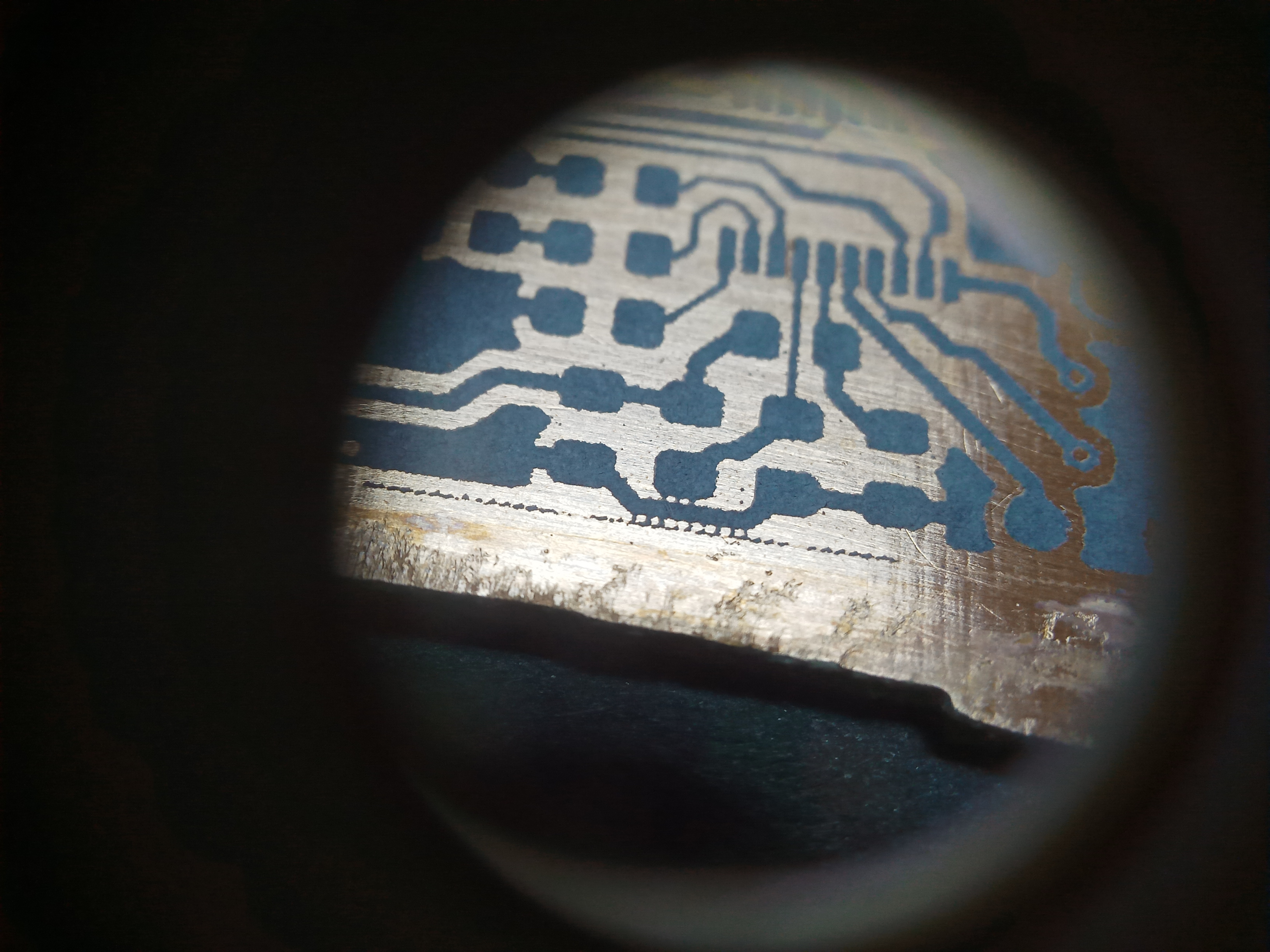
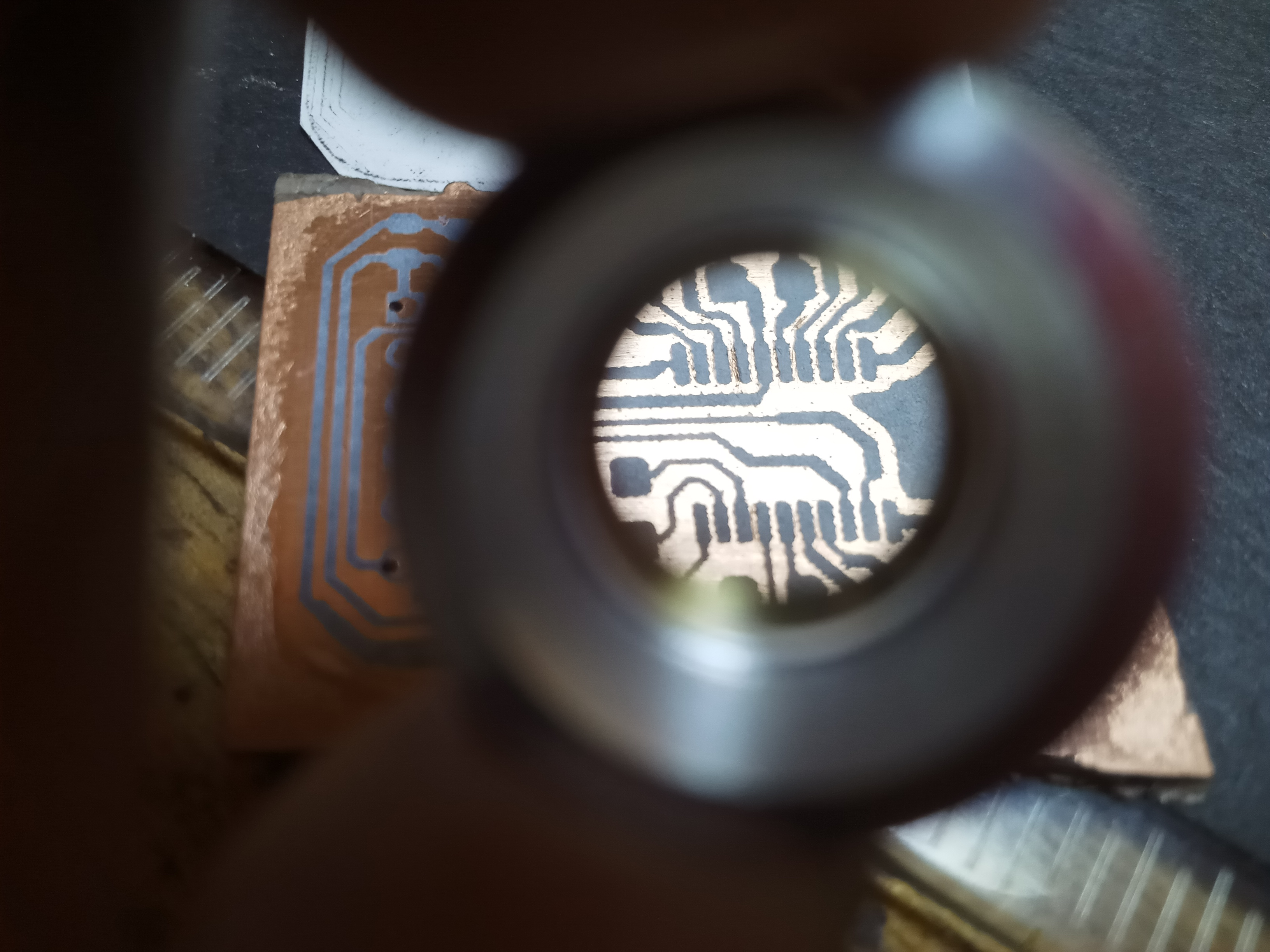
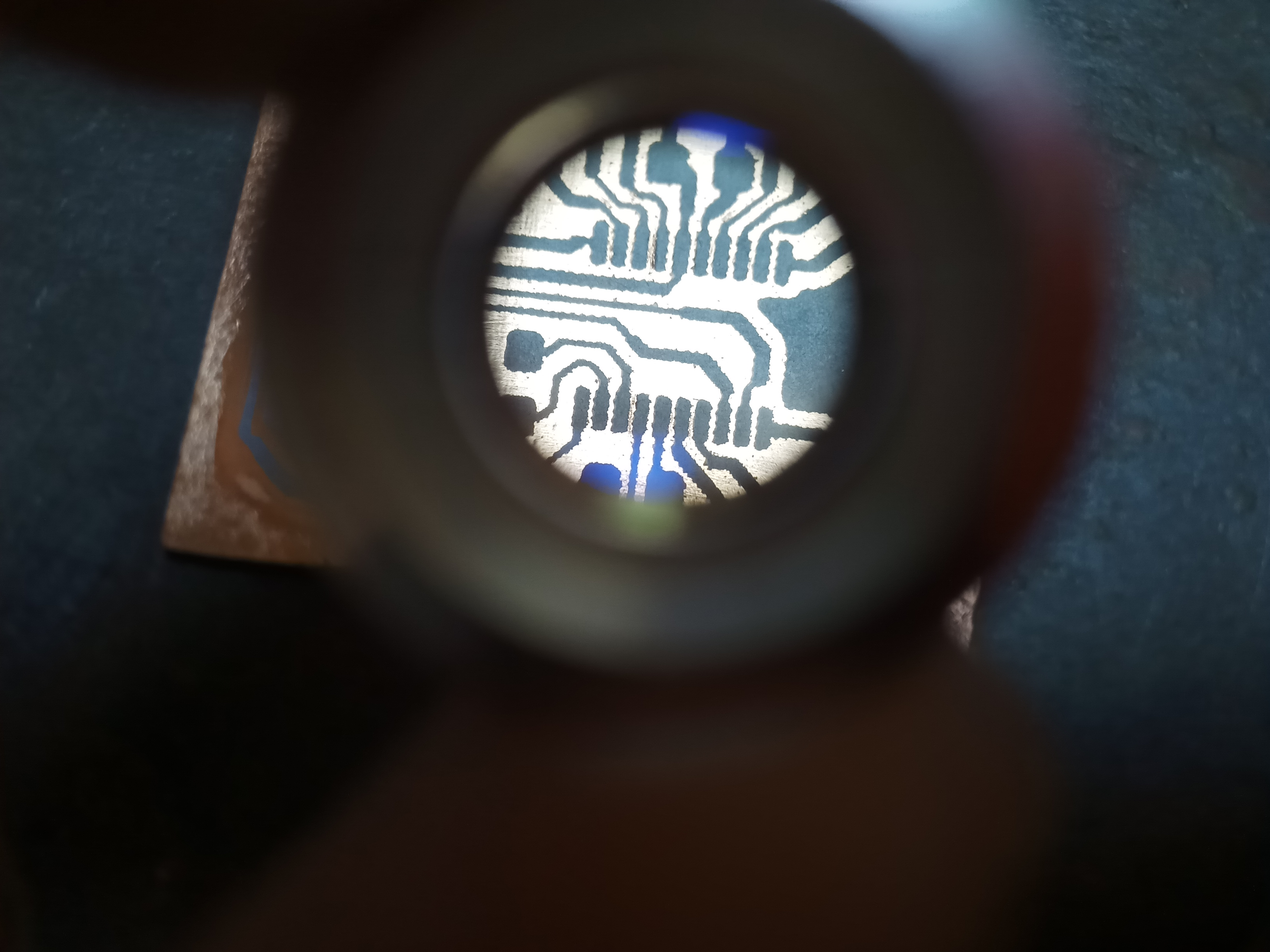
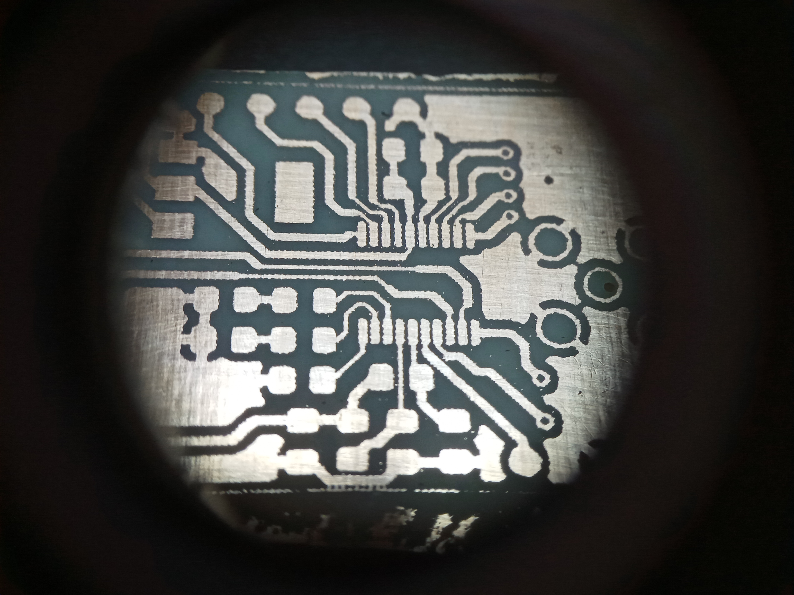
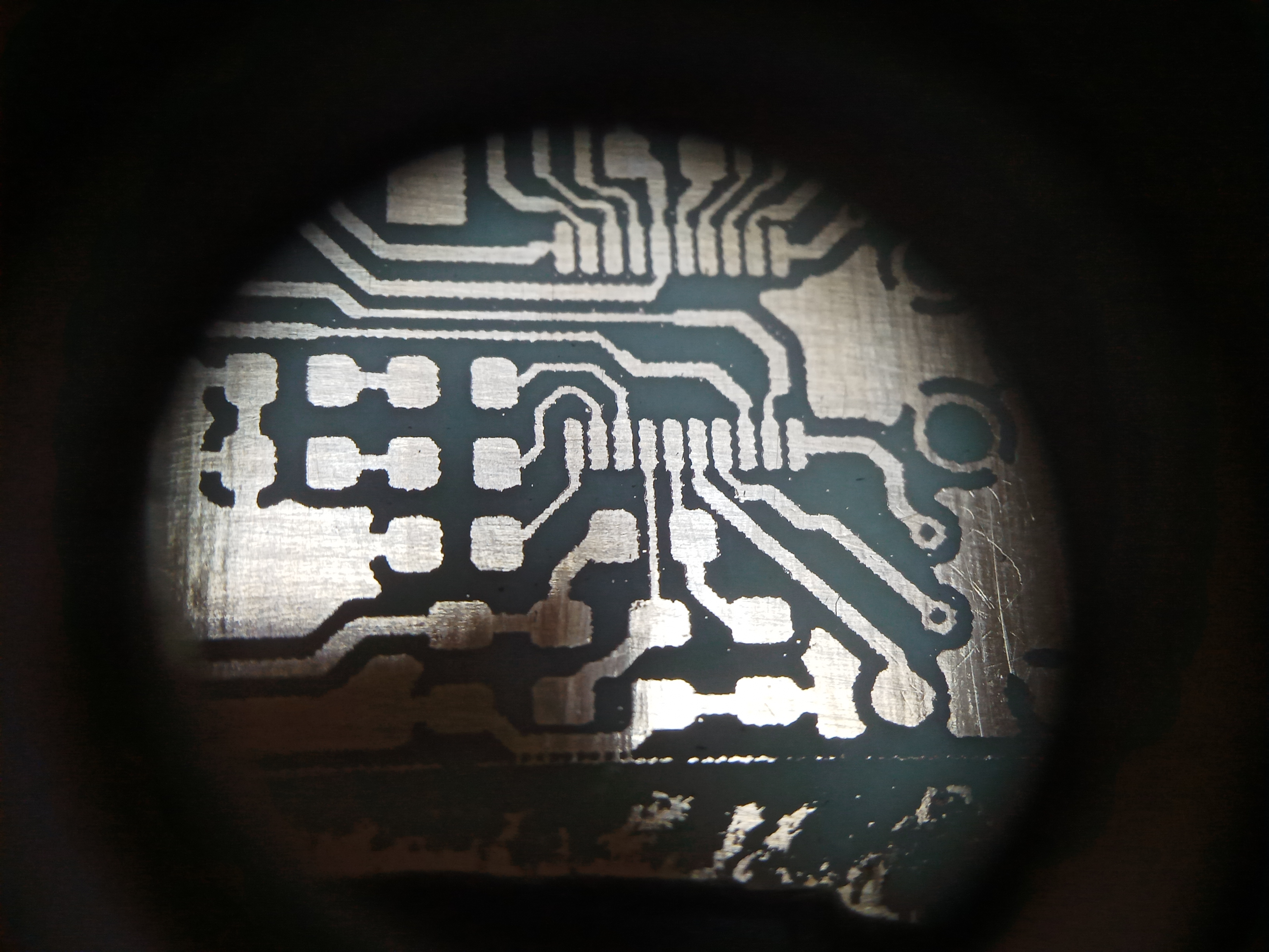
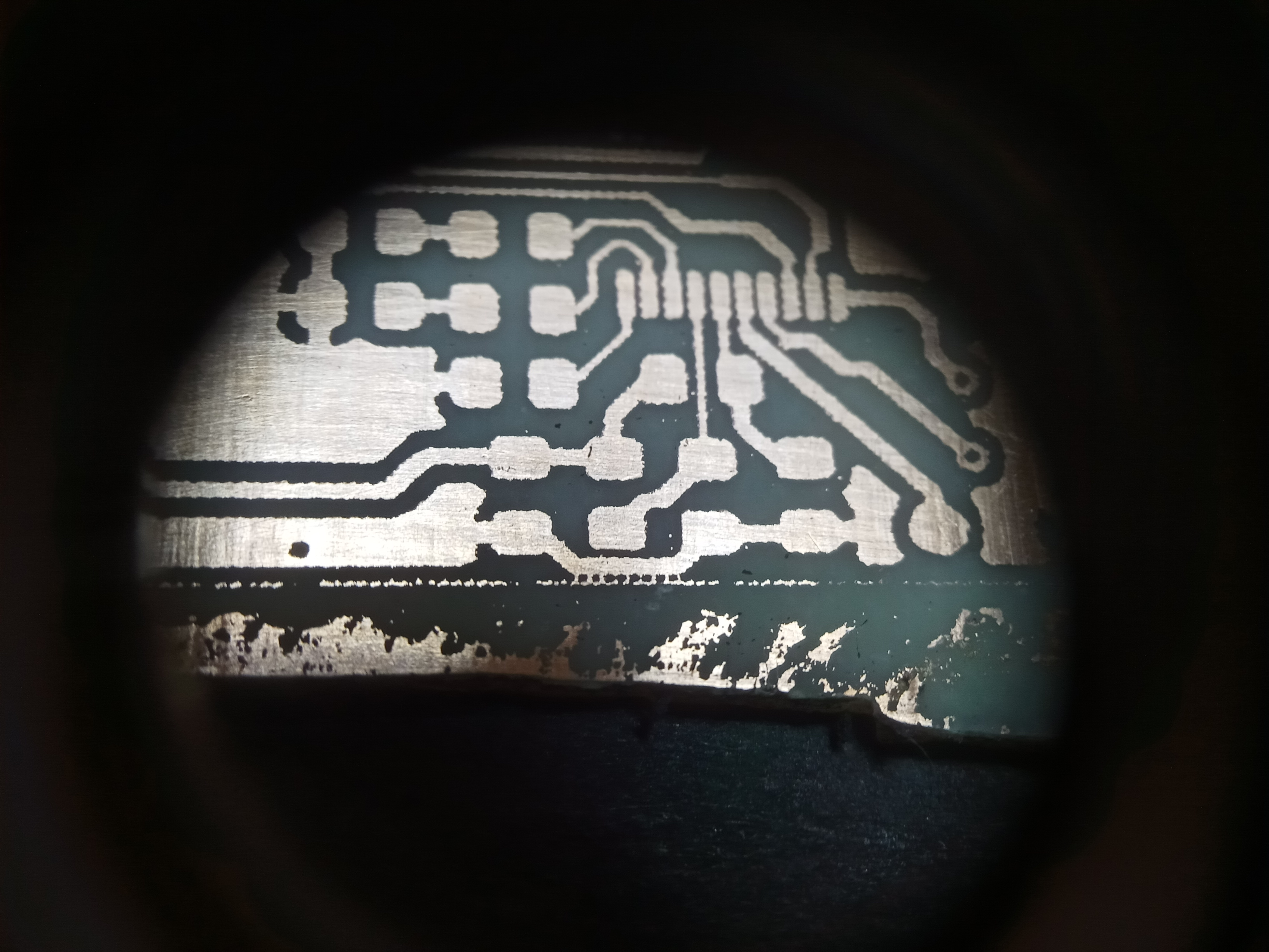
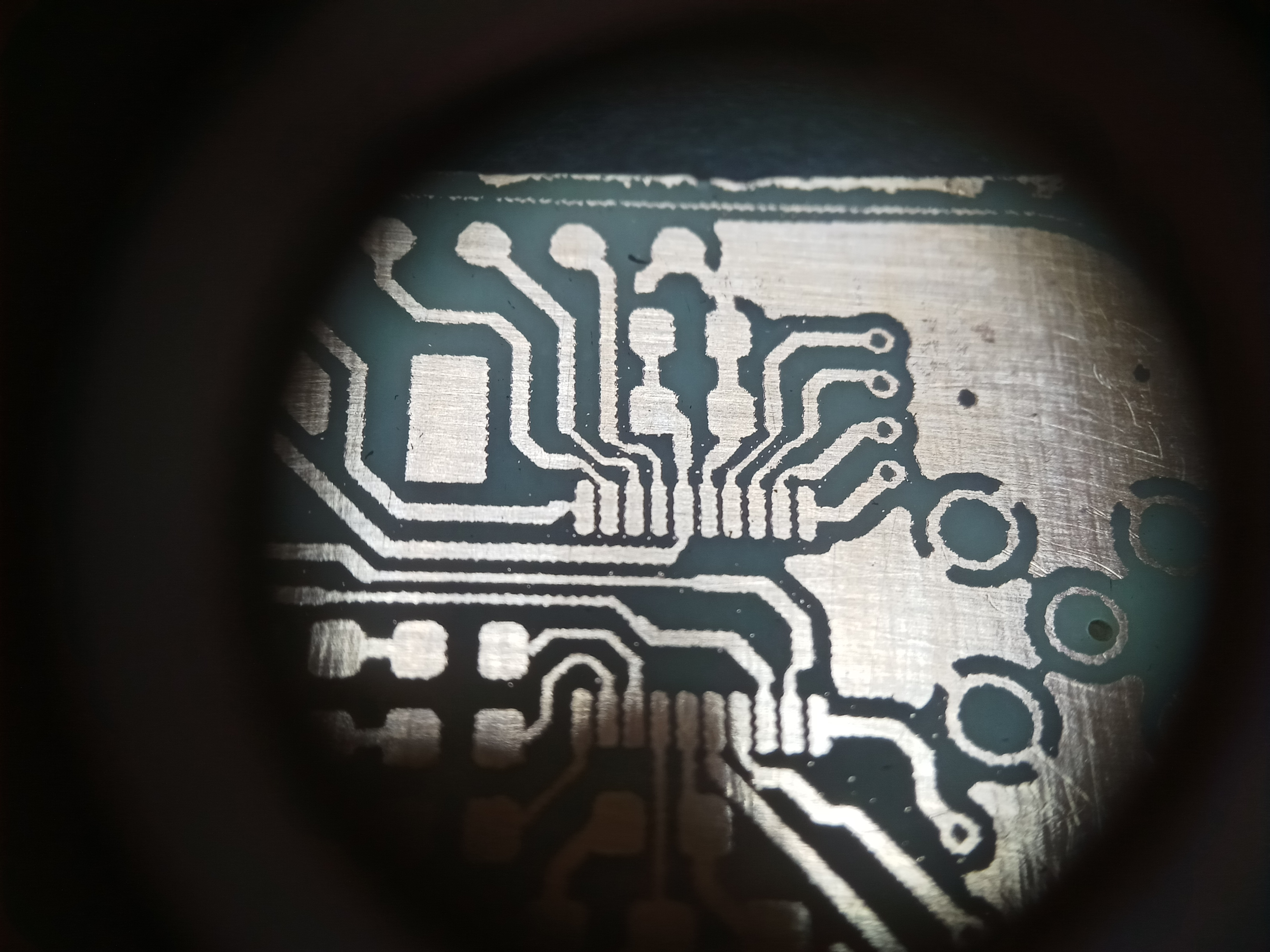
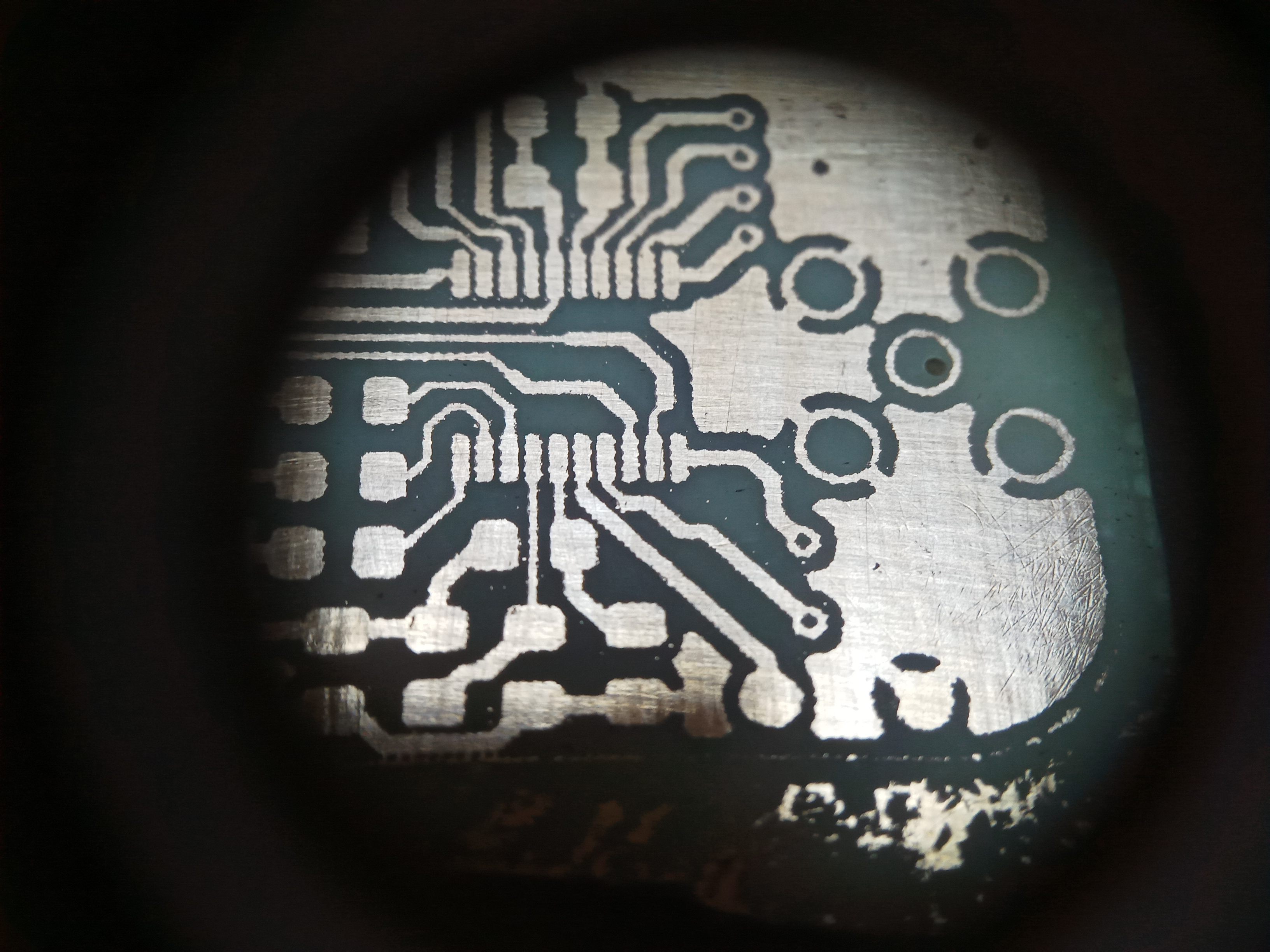
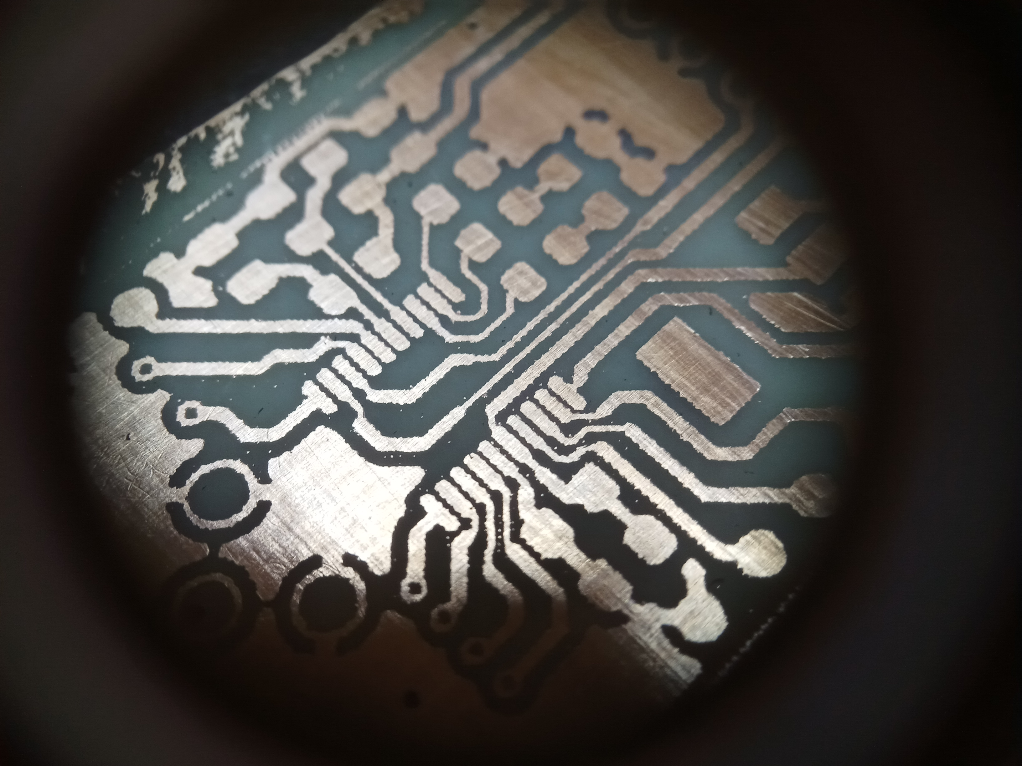
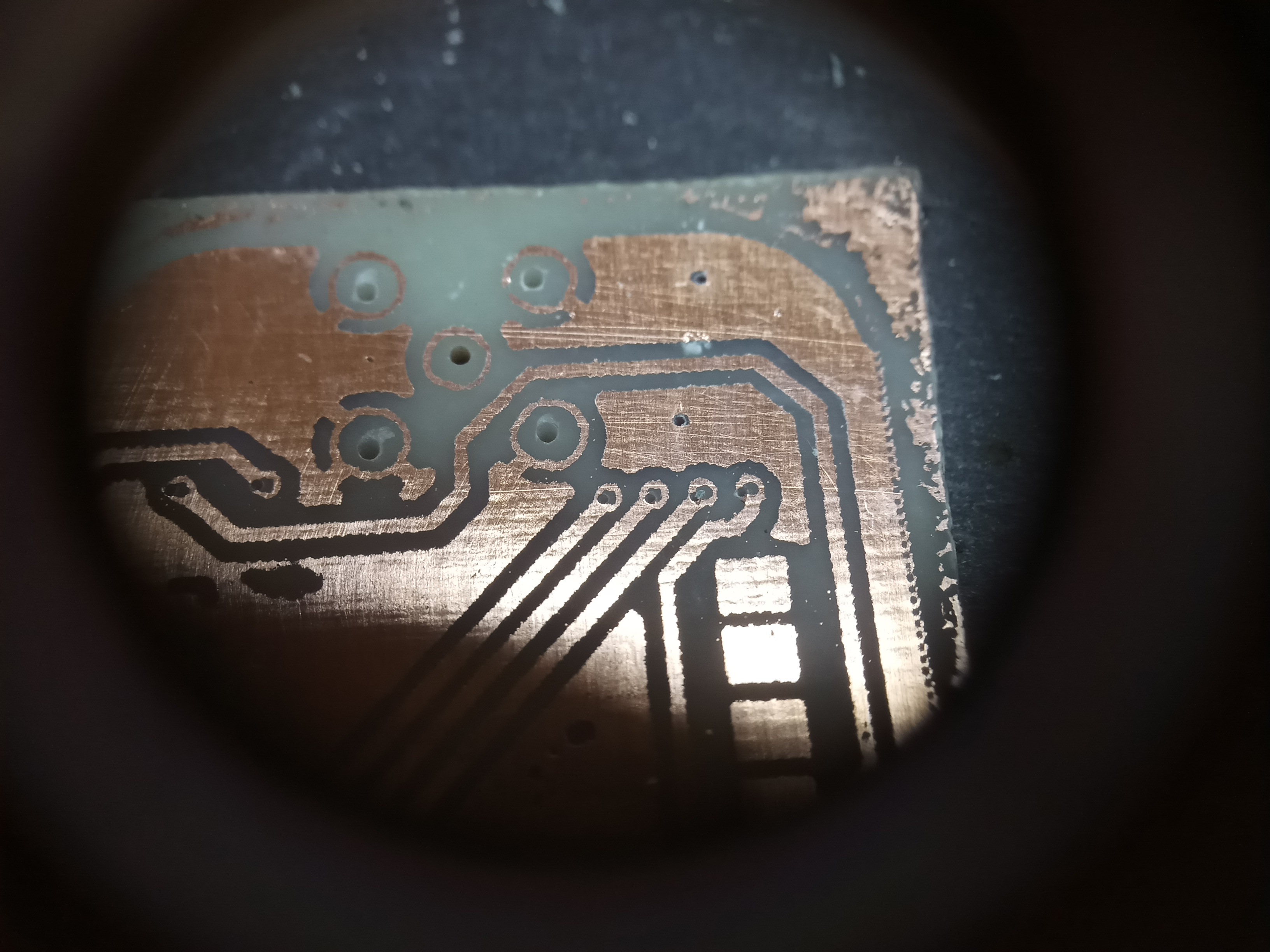
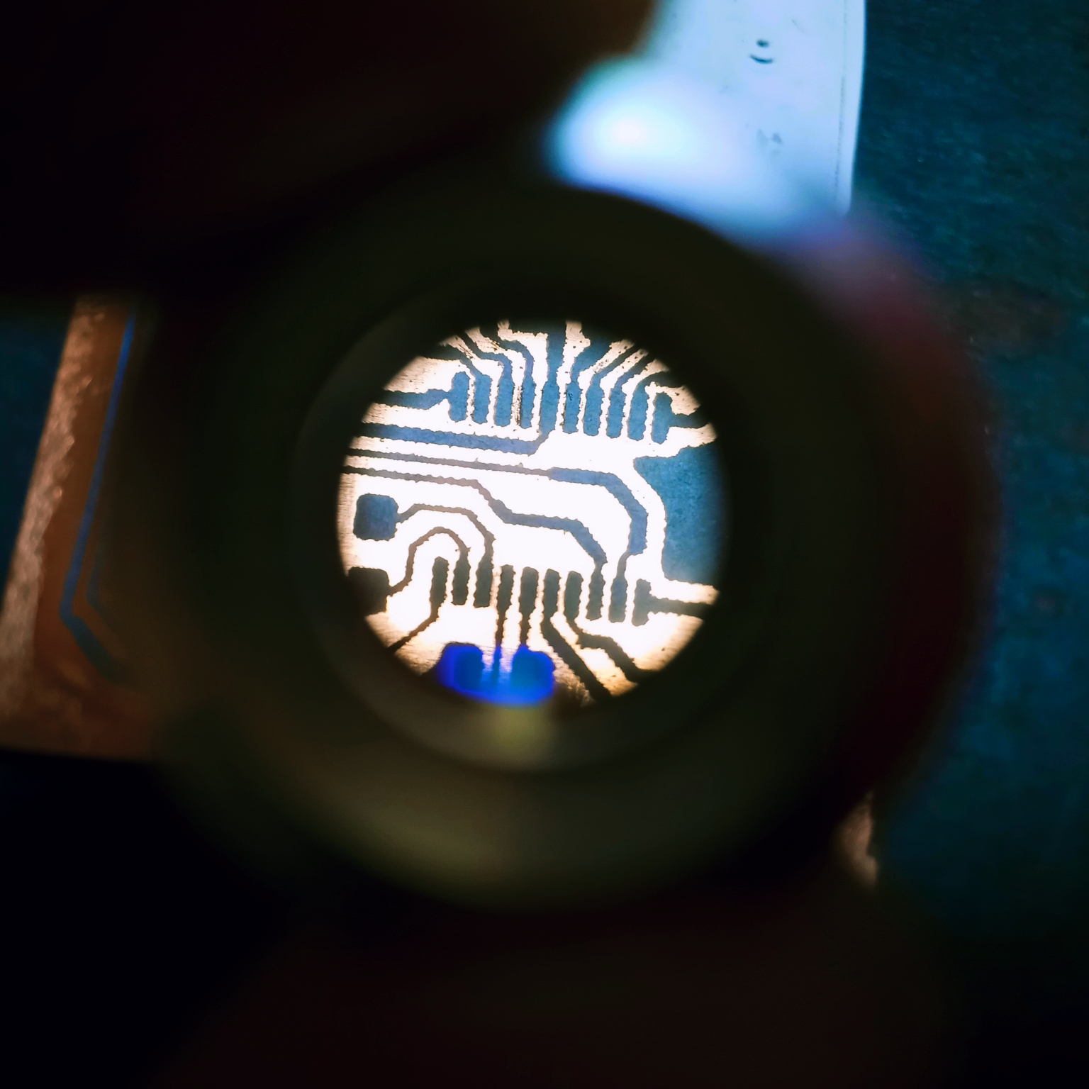
Since this side of the board has the most detail, I inspected it with the help of a lens I had lying around, using a scalpel to scrape away excess toner and permanent marker to close unbridged connections.
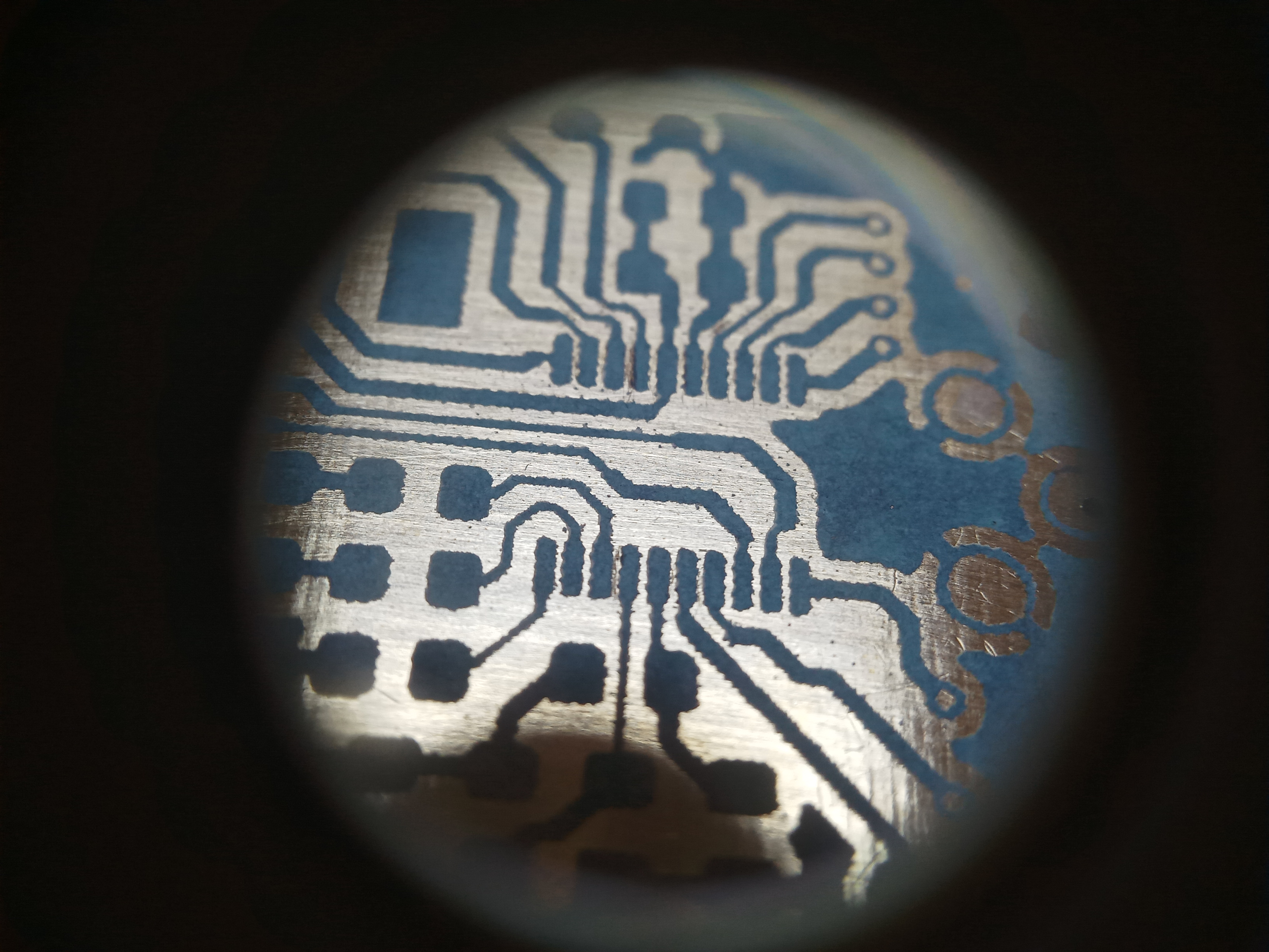
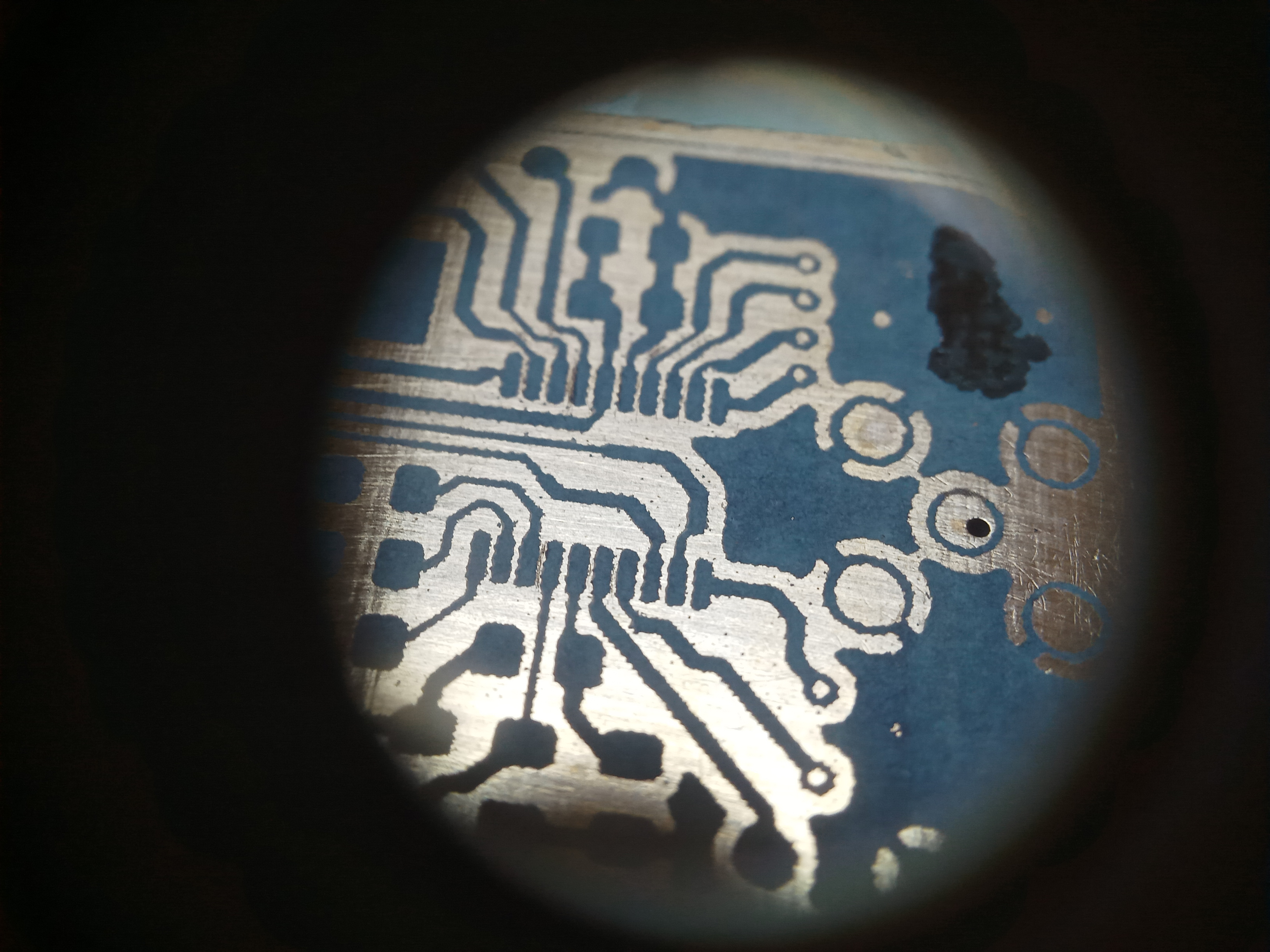
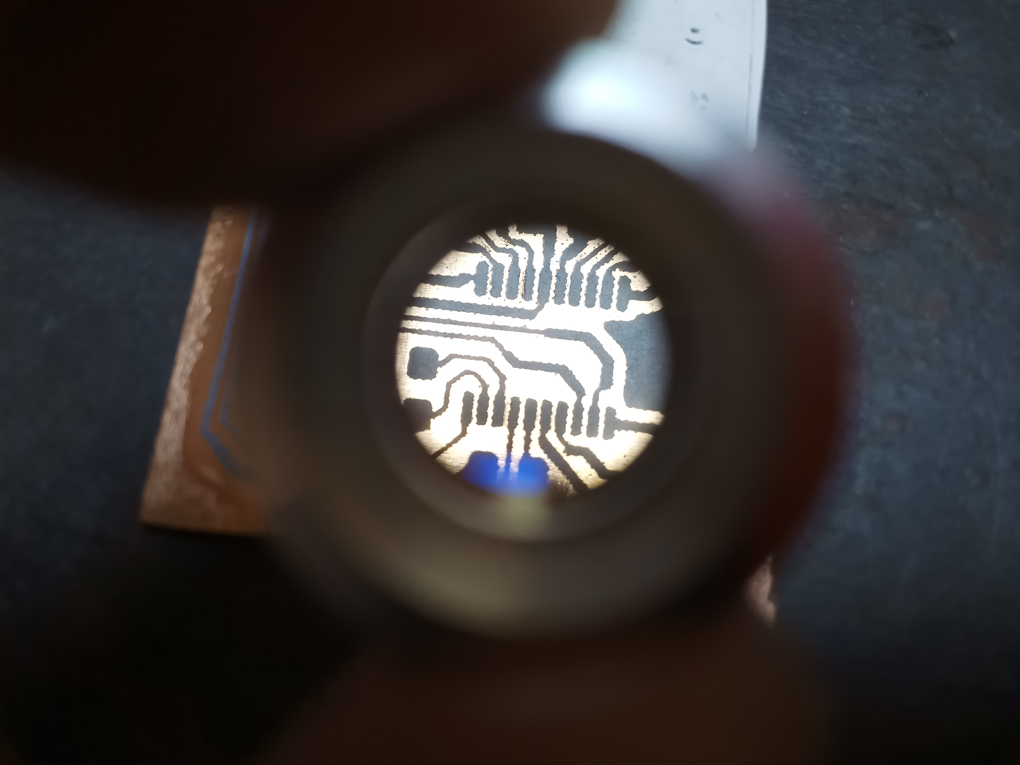
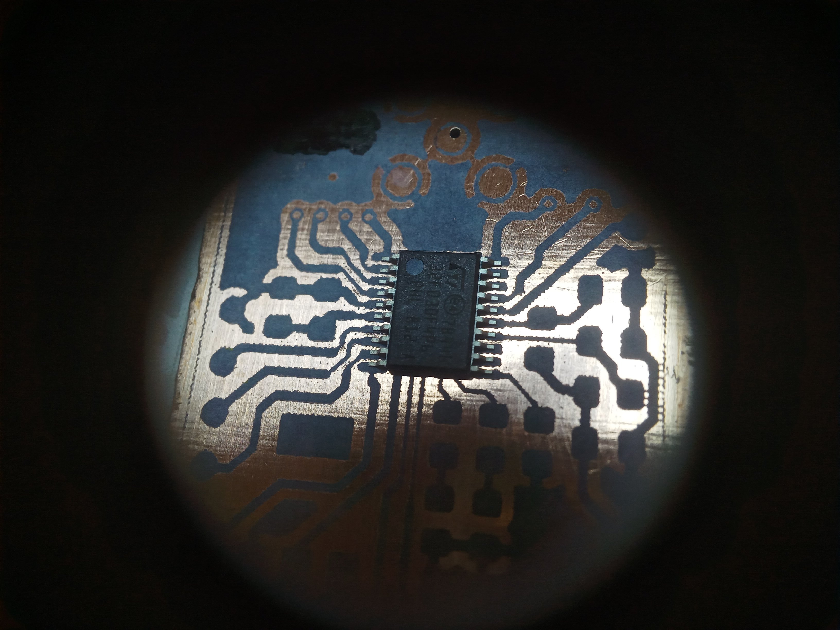
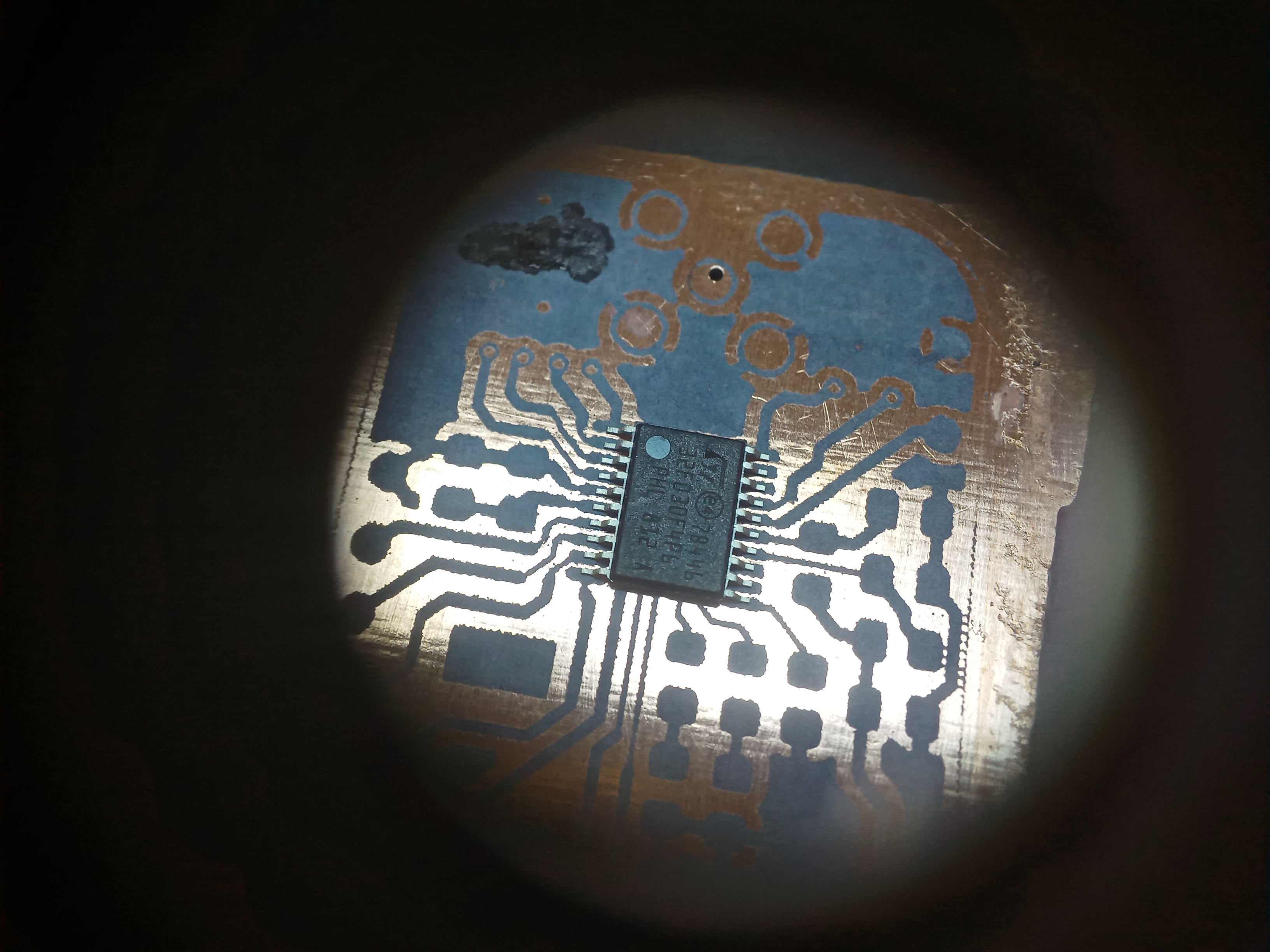
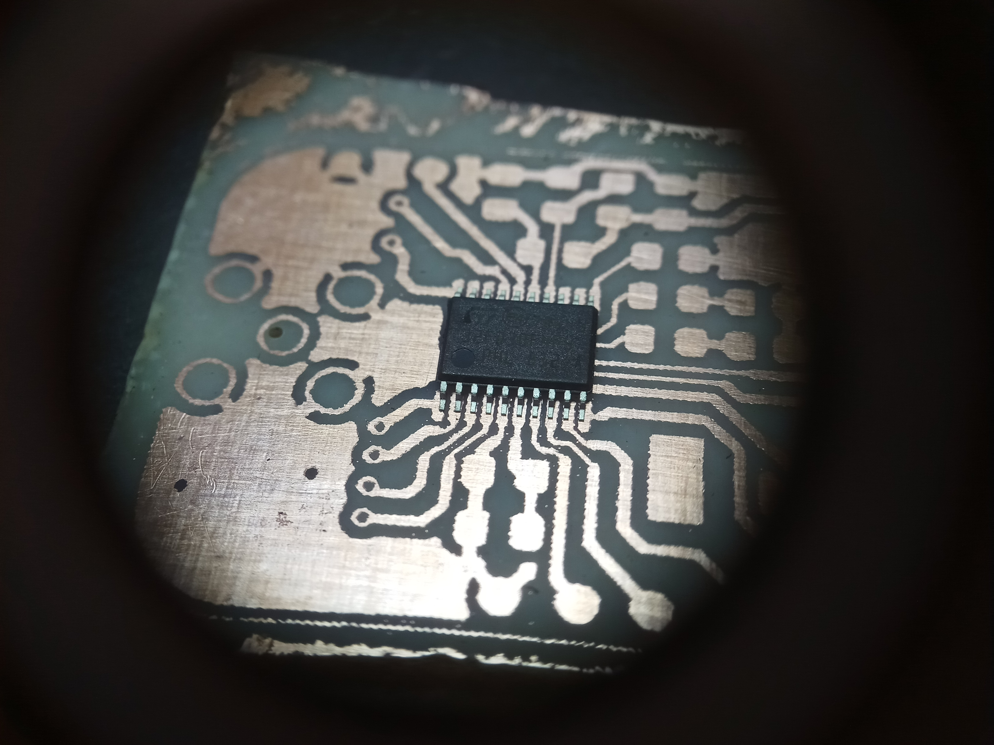
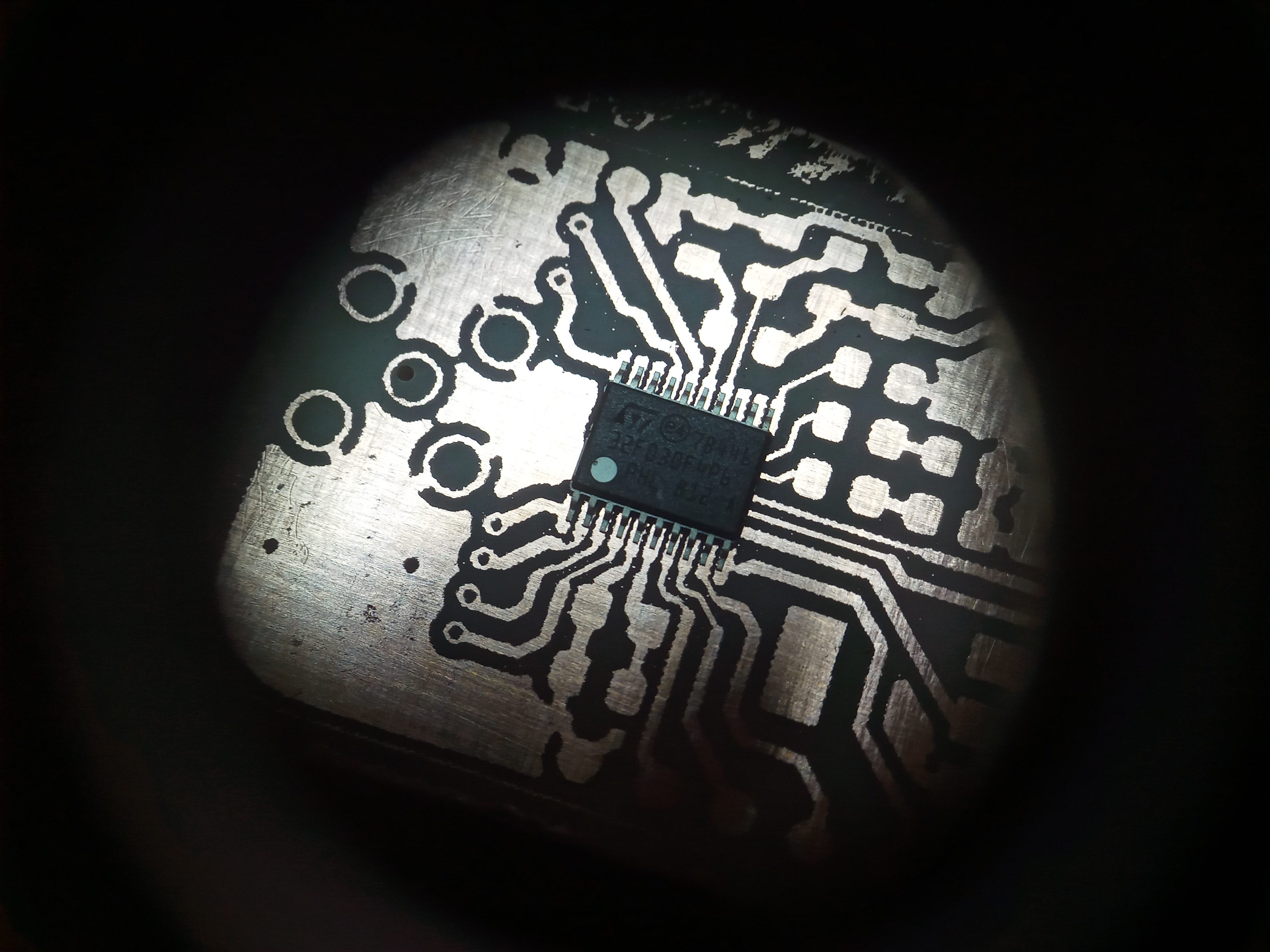
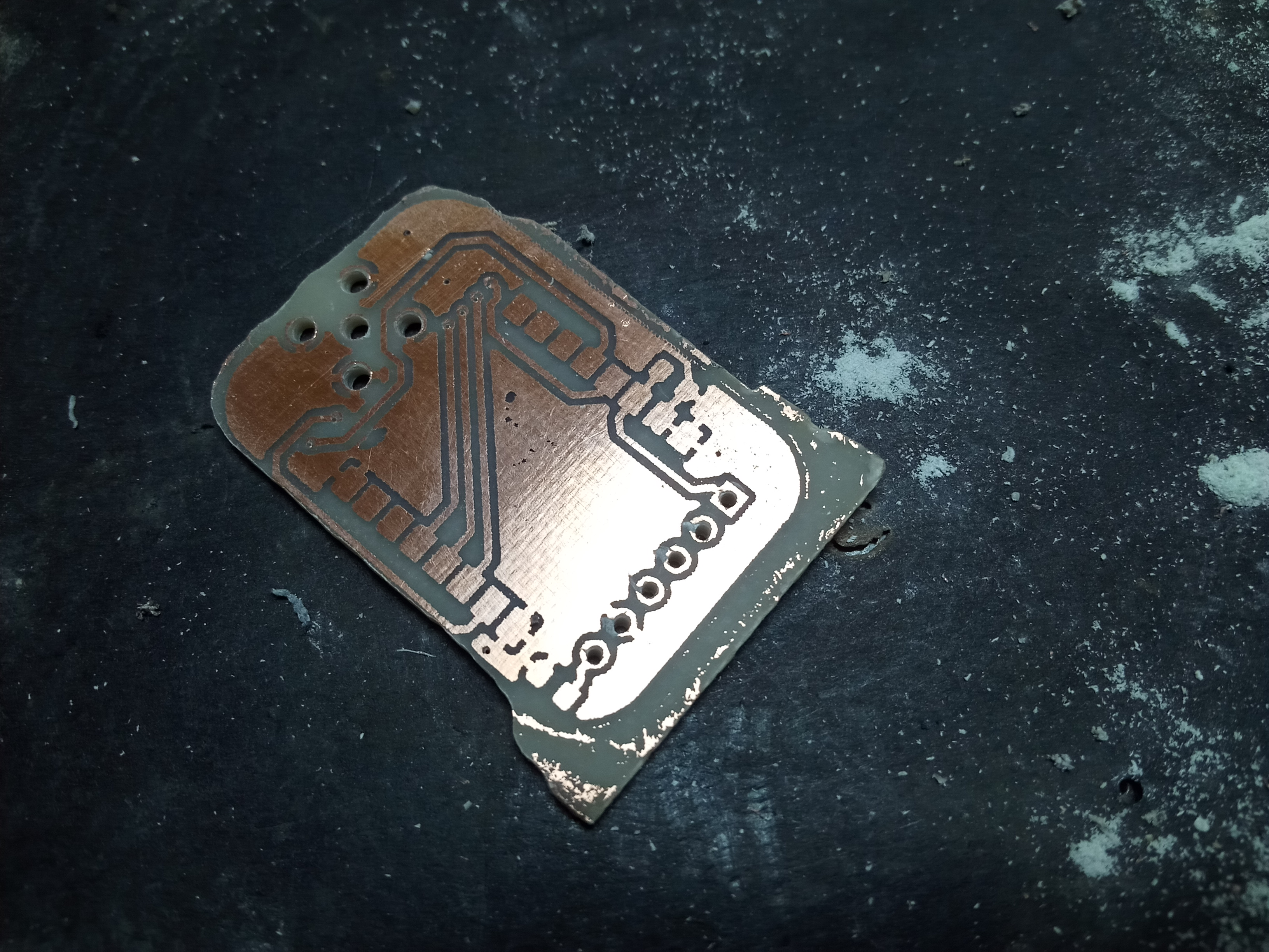
I also tried out one of the components for a test fit.
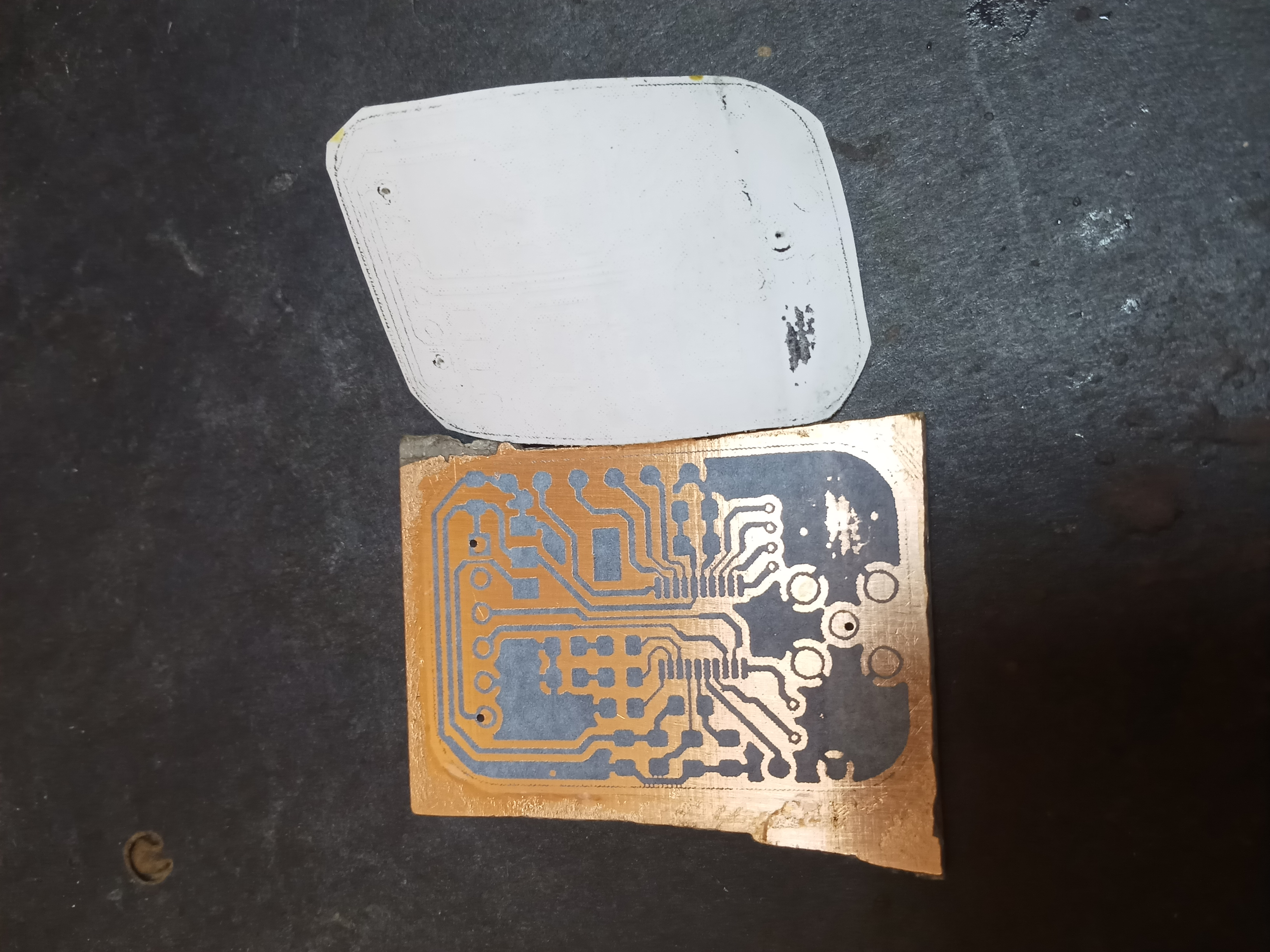
Etching the Bottom layer
Safery Warning:
- Make sure you conduct this part of the procedure in a well-ventilated area away from sources of fire as significant acetone inhalation is known to cause health problems.
- Acetone is a strong solvent and although it will not have much of an effect on your skin, it WILL dissolve plastic especially ABS, which is the type of plastic used to make casings for most electronic devices.

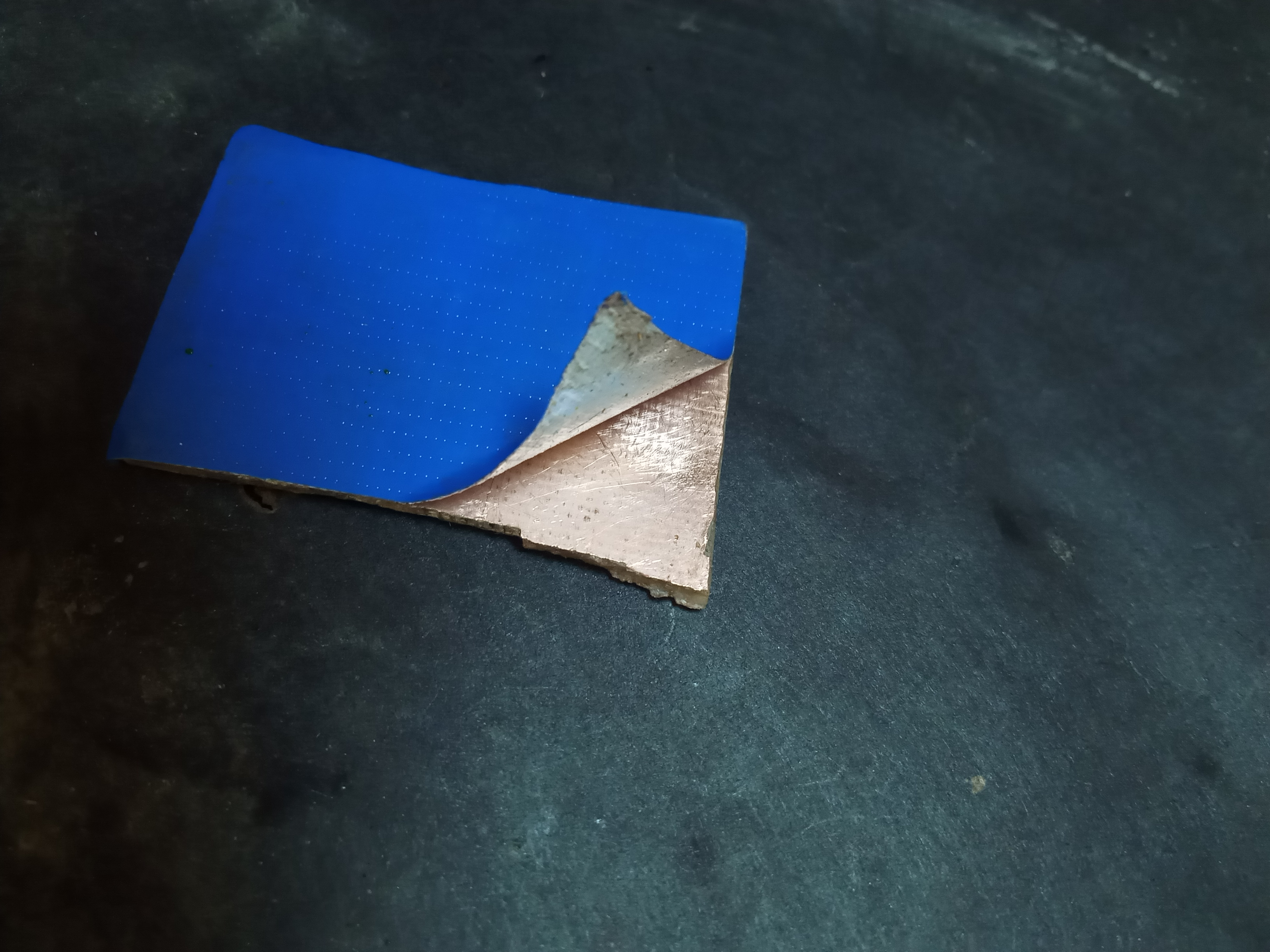
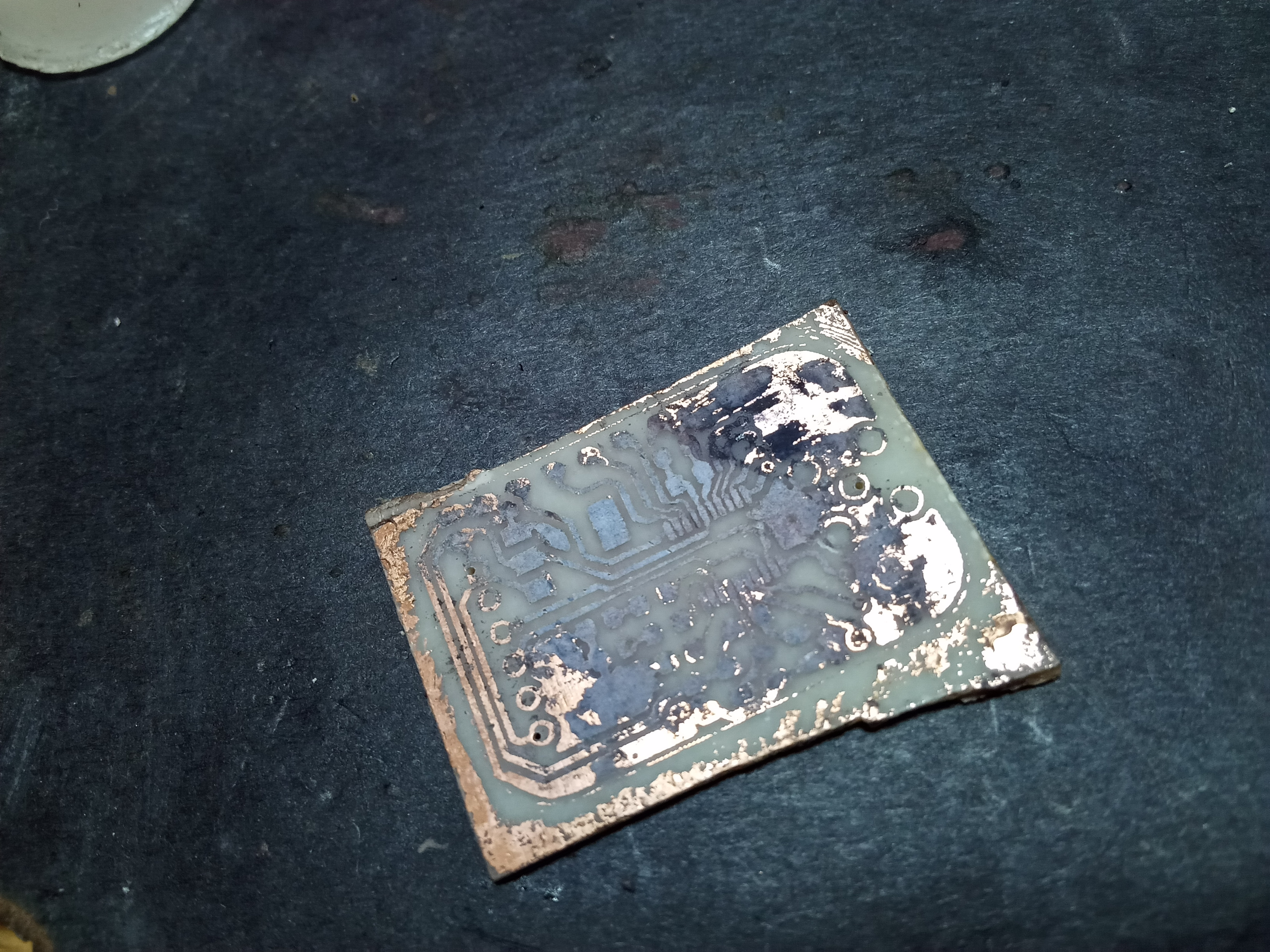
Before etching the bottom layer, remember to protect the top layer with waterproof tape.
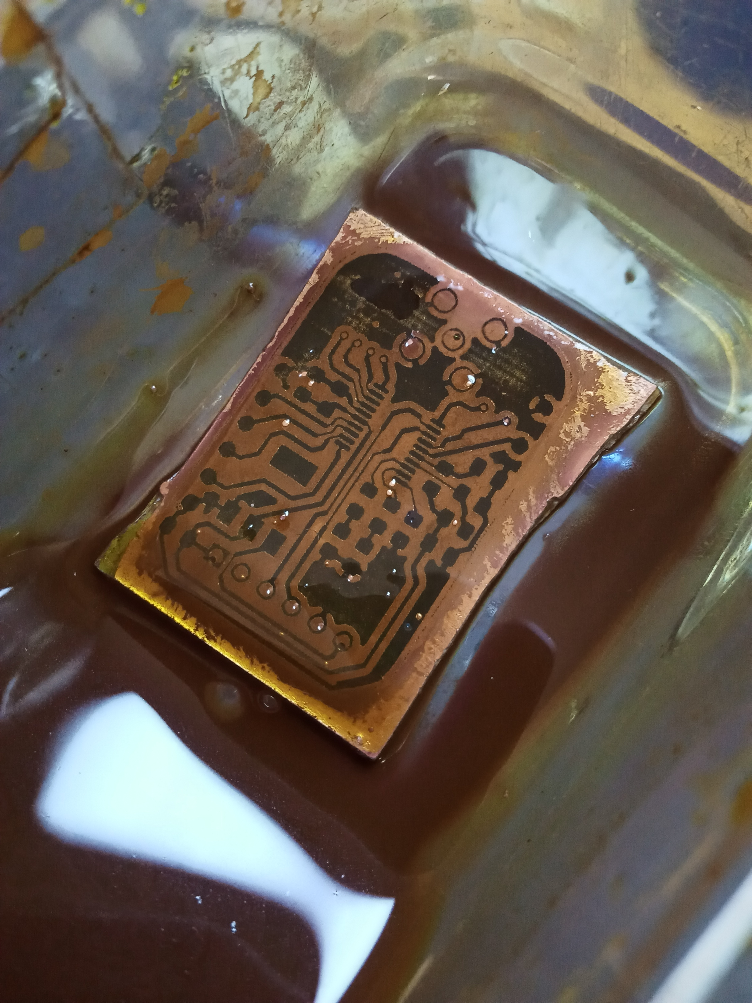
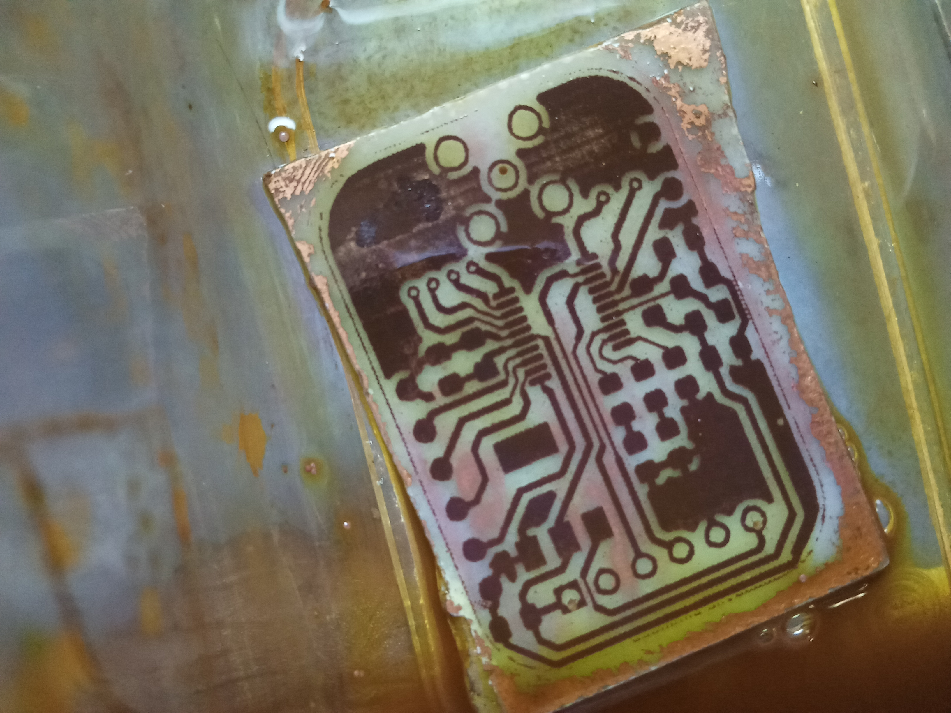
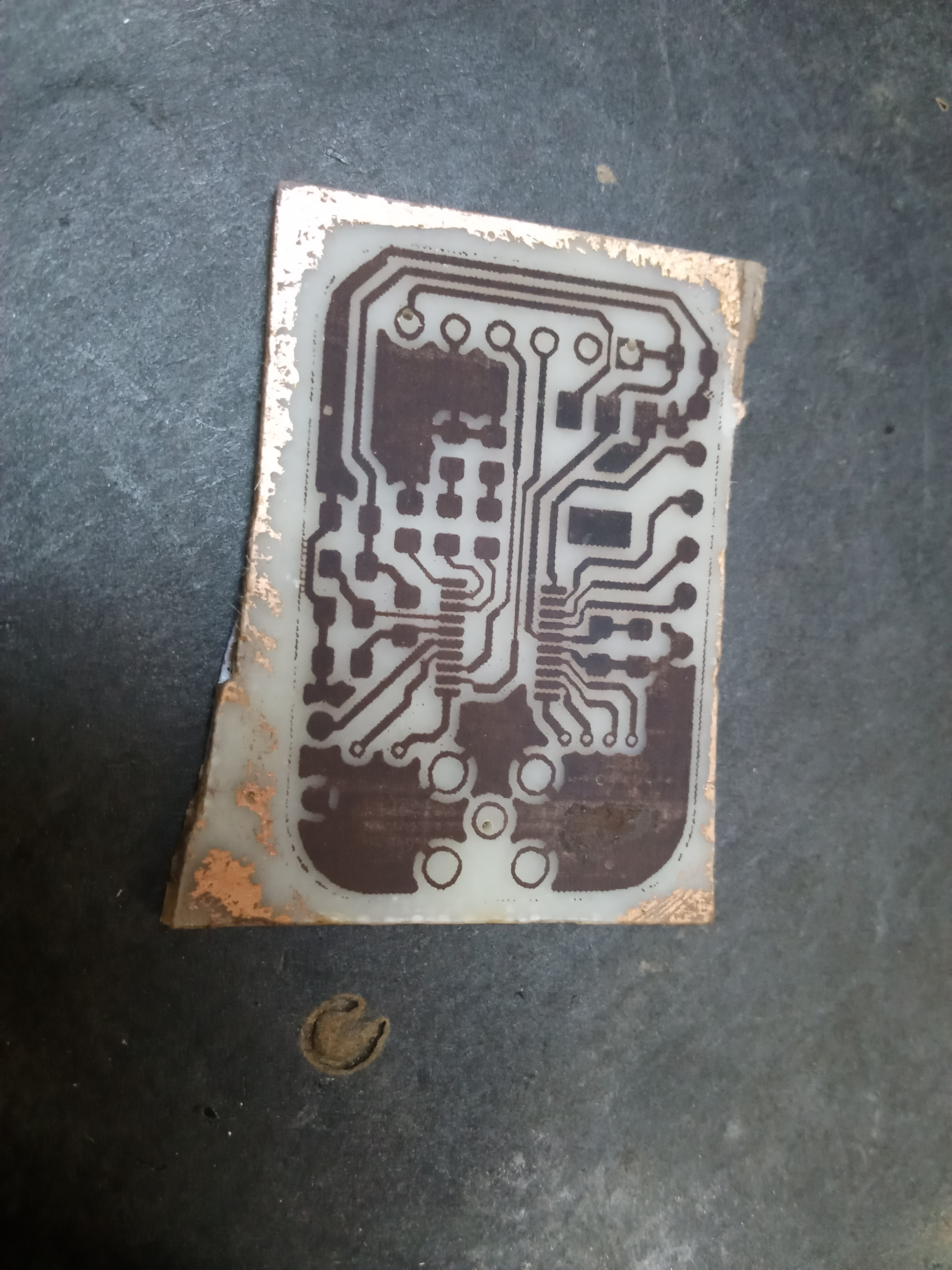
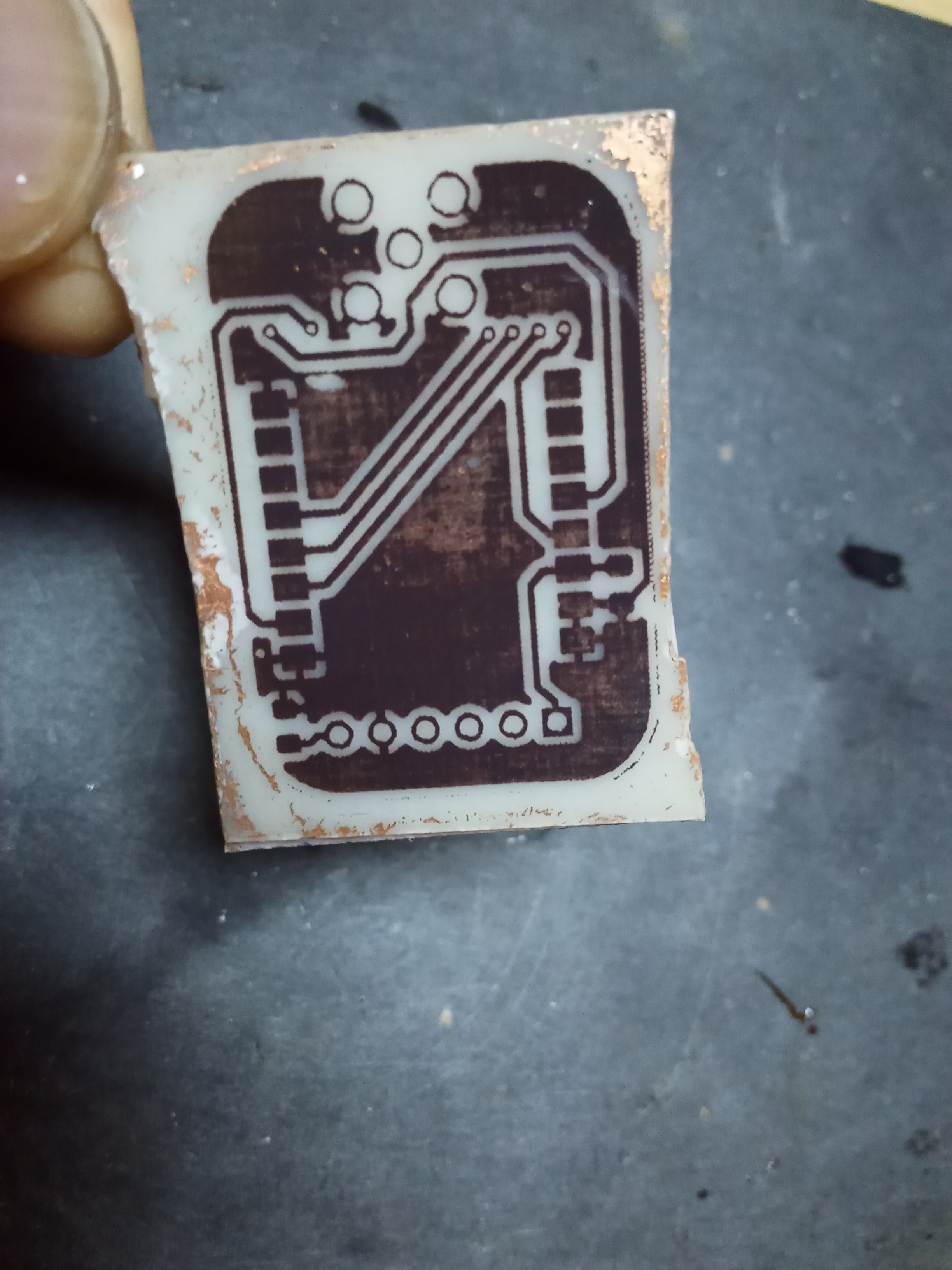
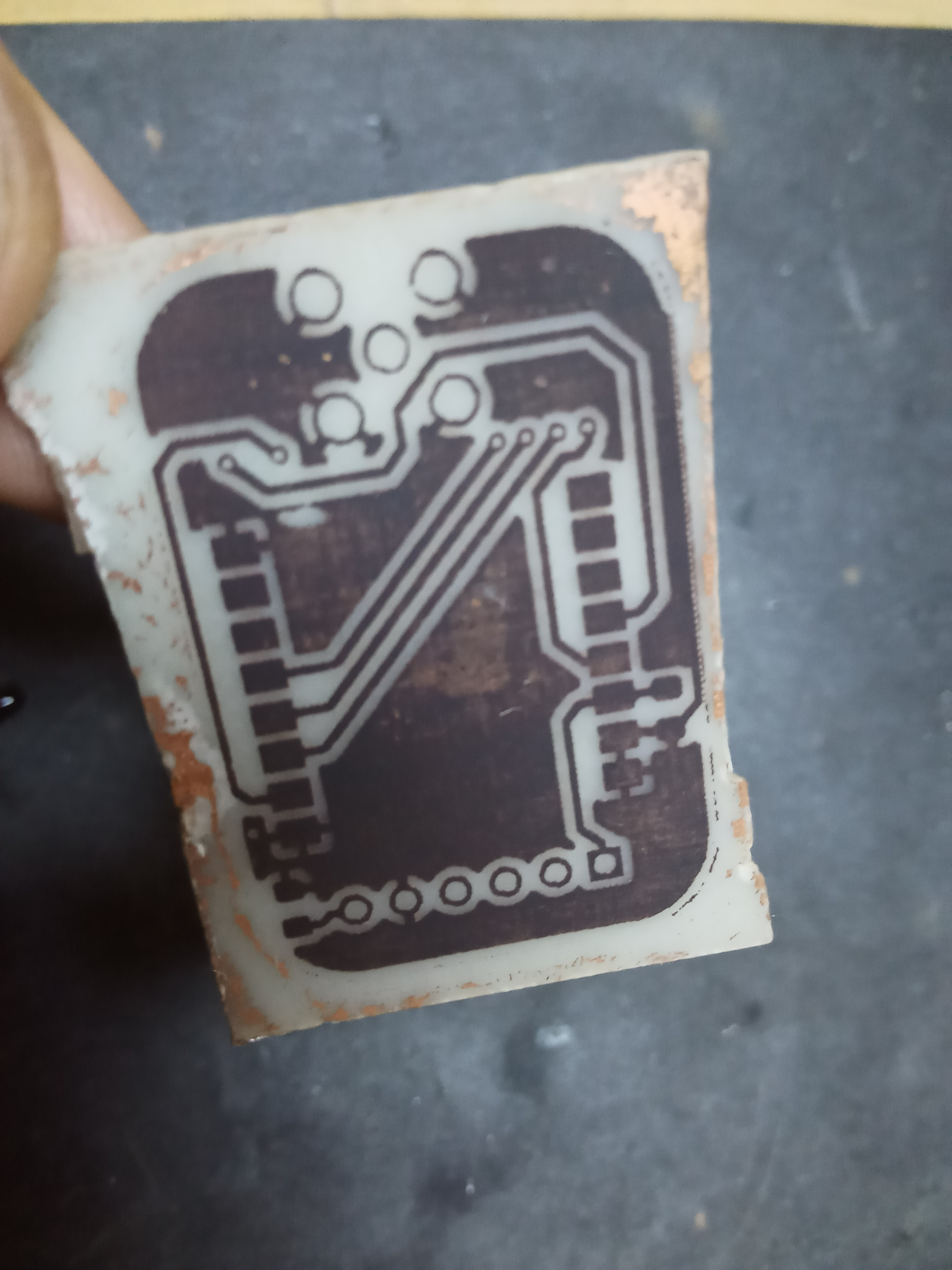
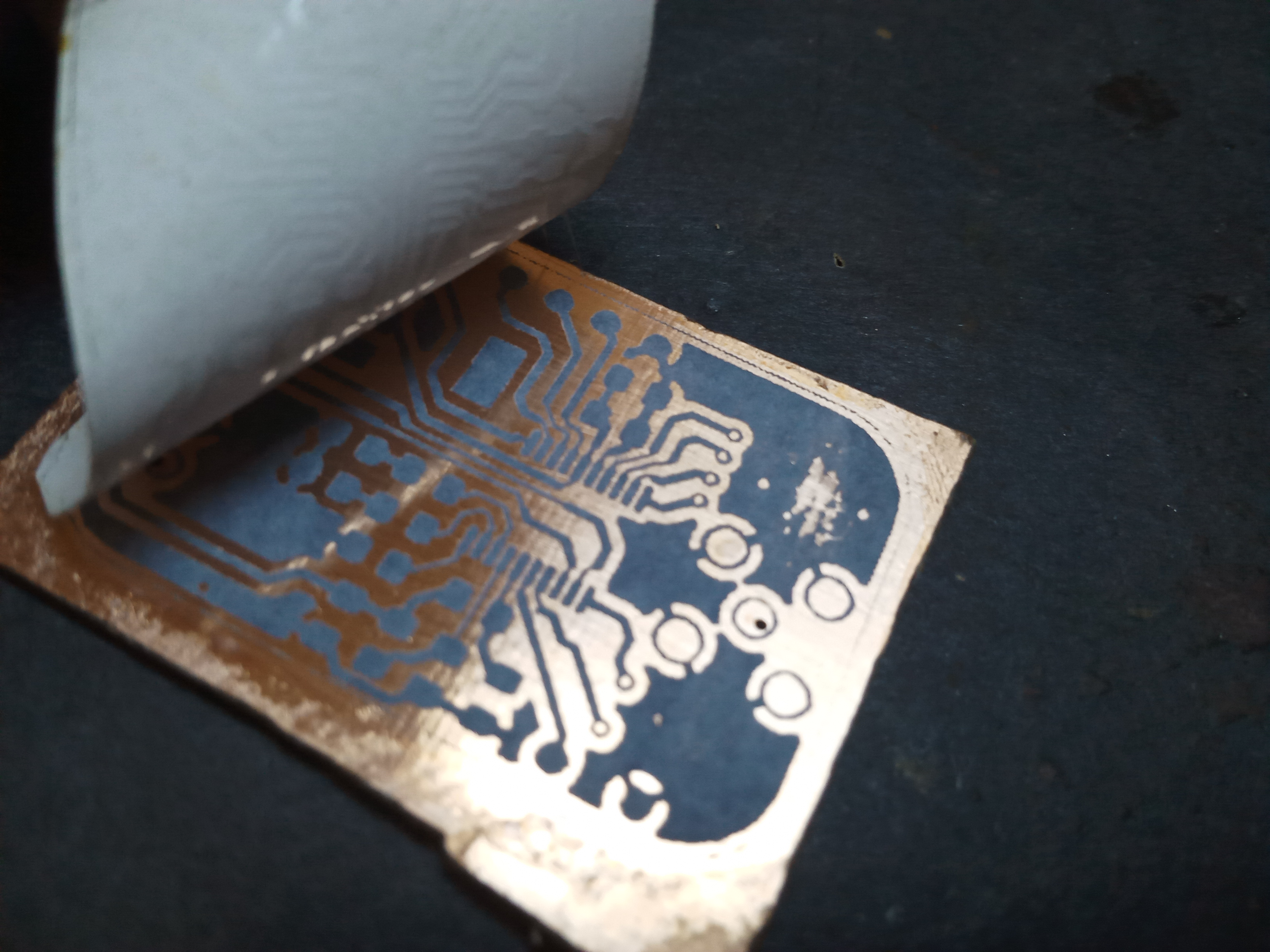
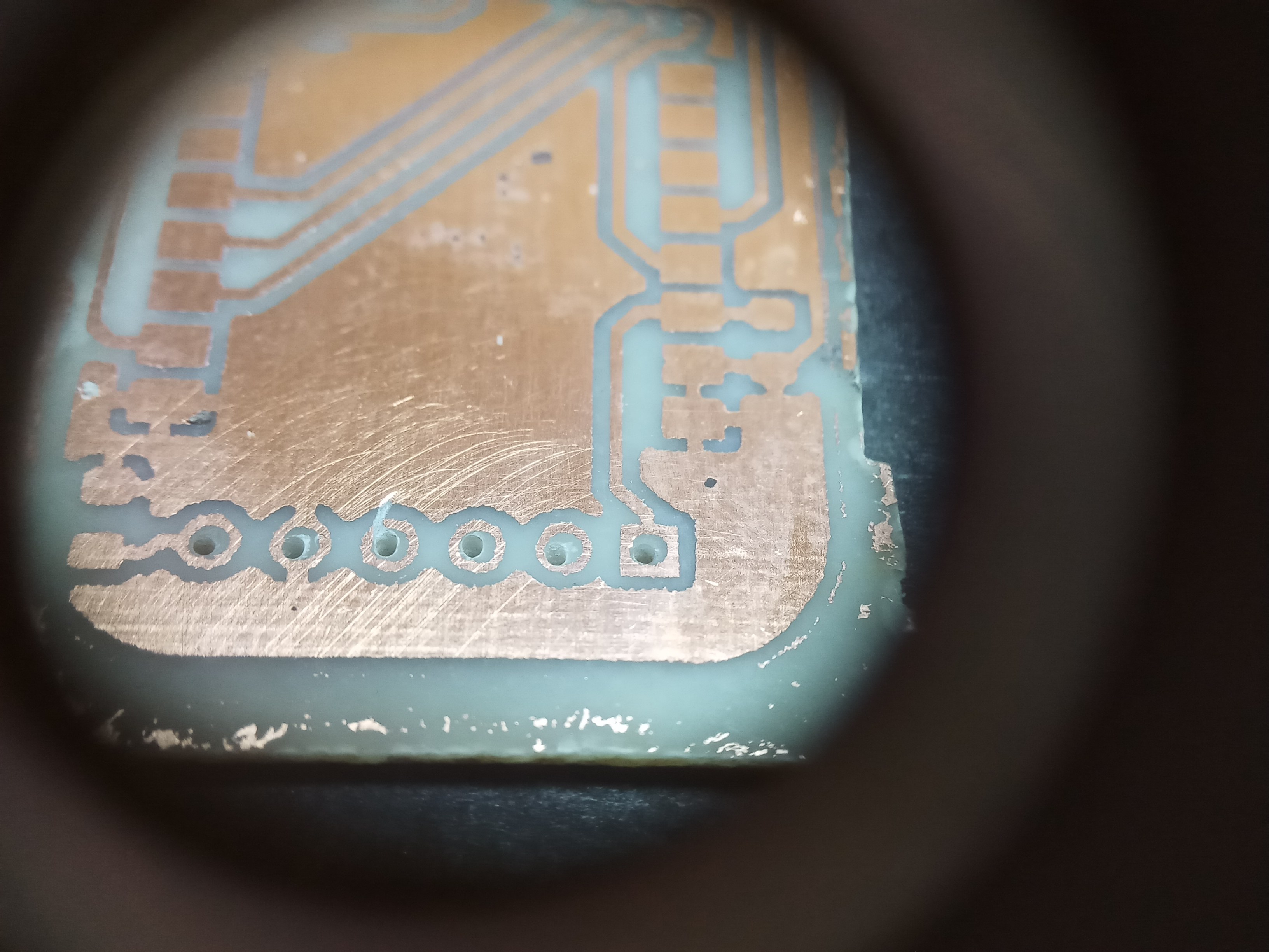
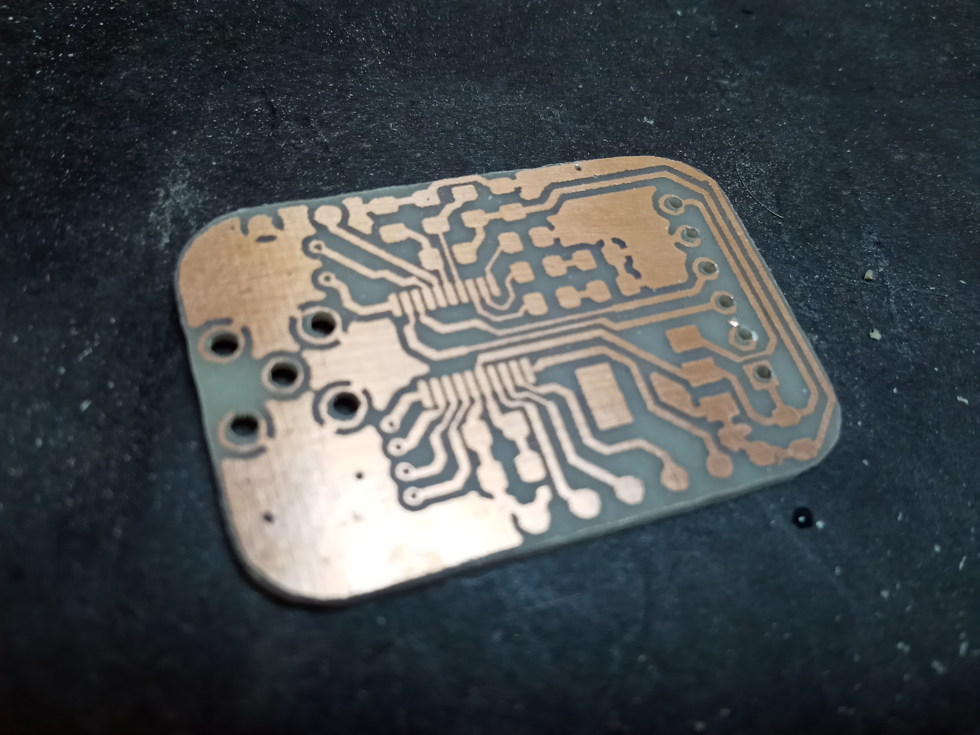
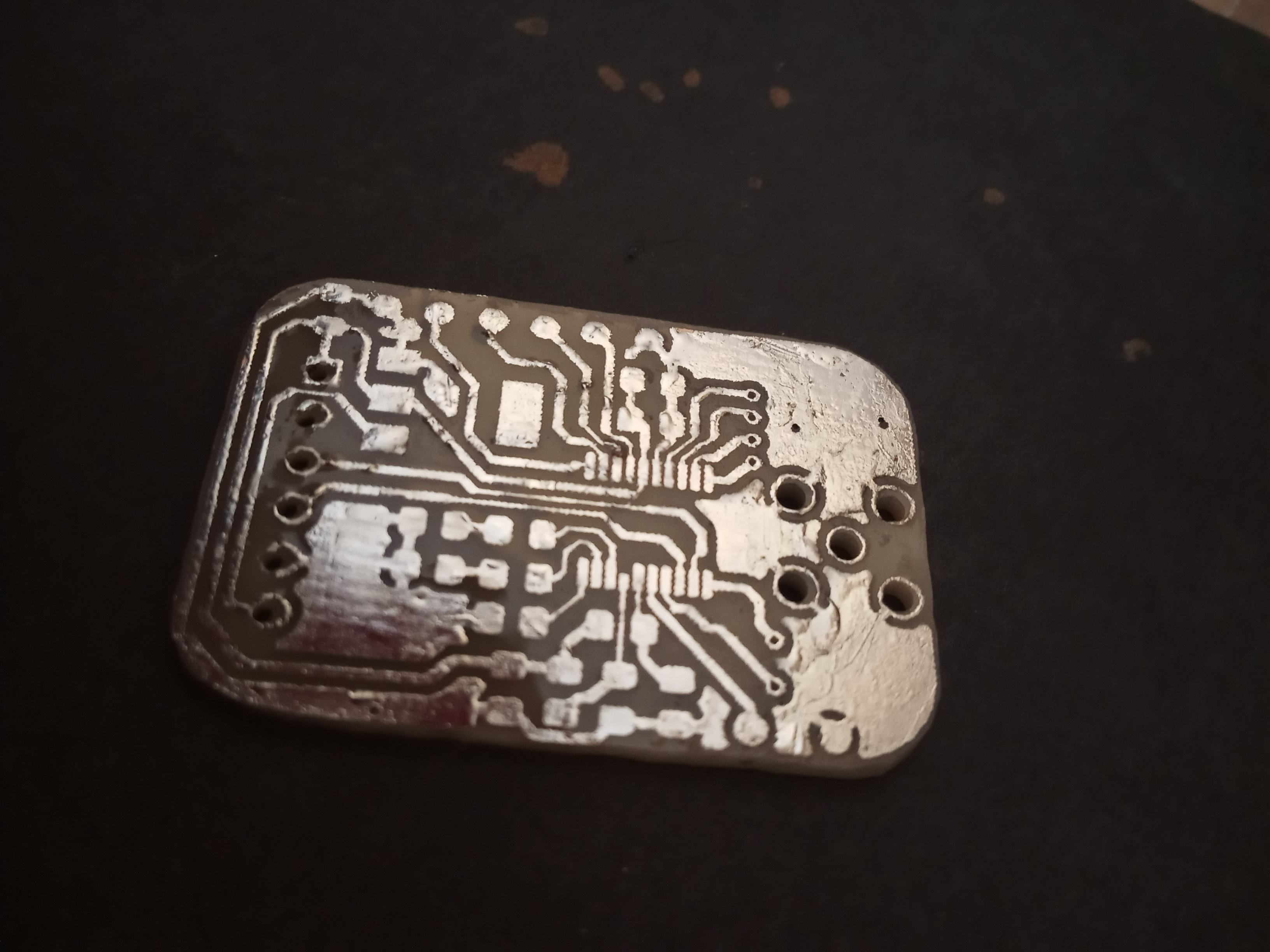
And it is time for the big reveal; getting the toner off so we can see the work of our hands in its full glory. The most convenient method wipe with acetone (nail polish remover) which dissolves toner as well as any remnants of glue from previous processes.
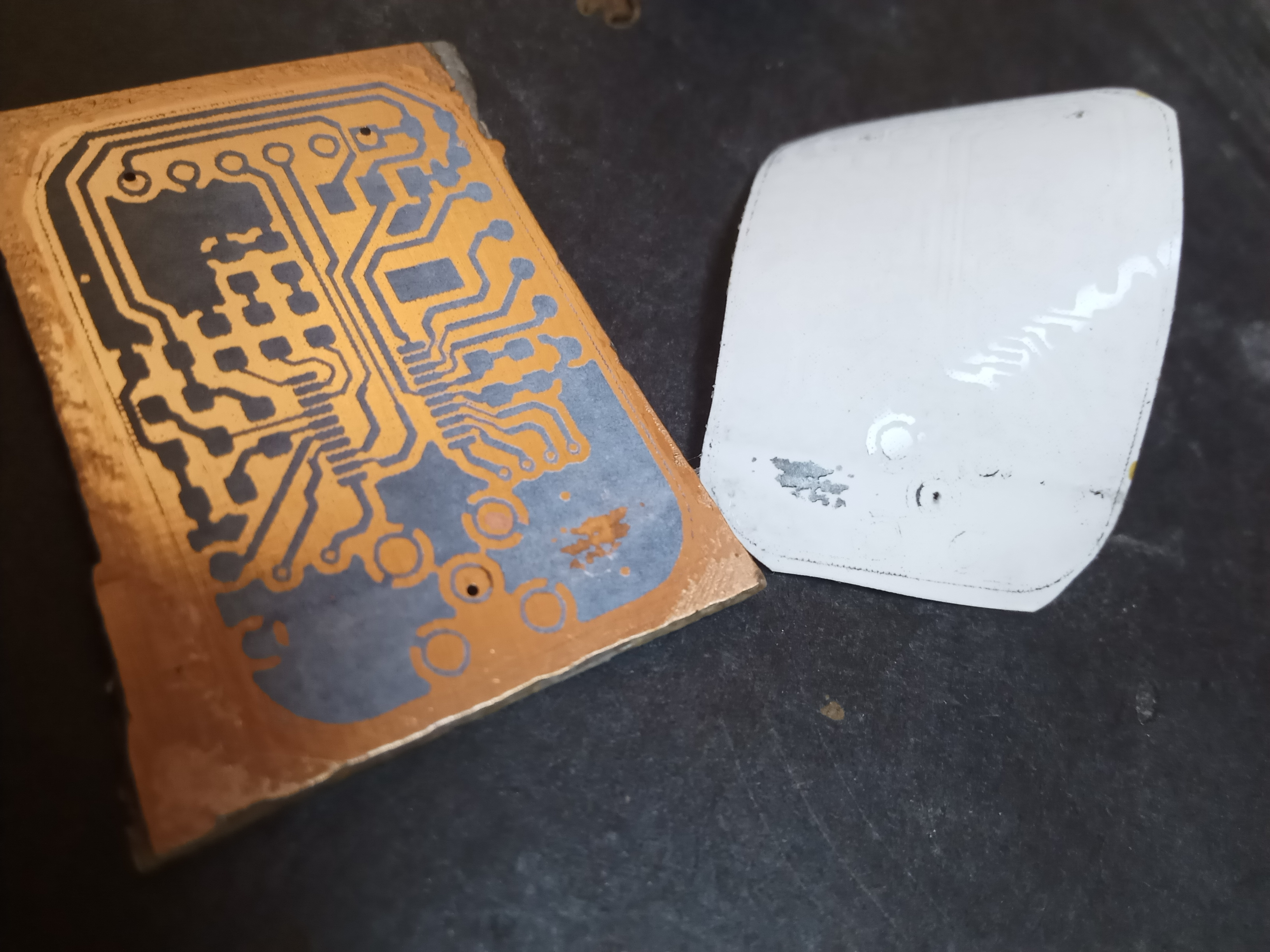
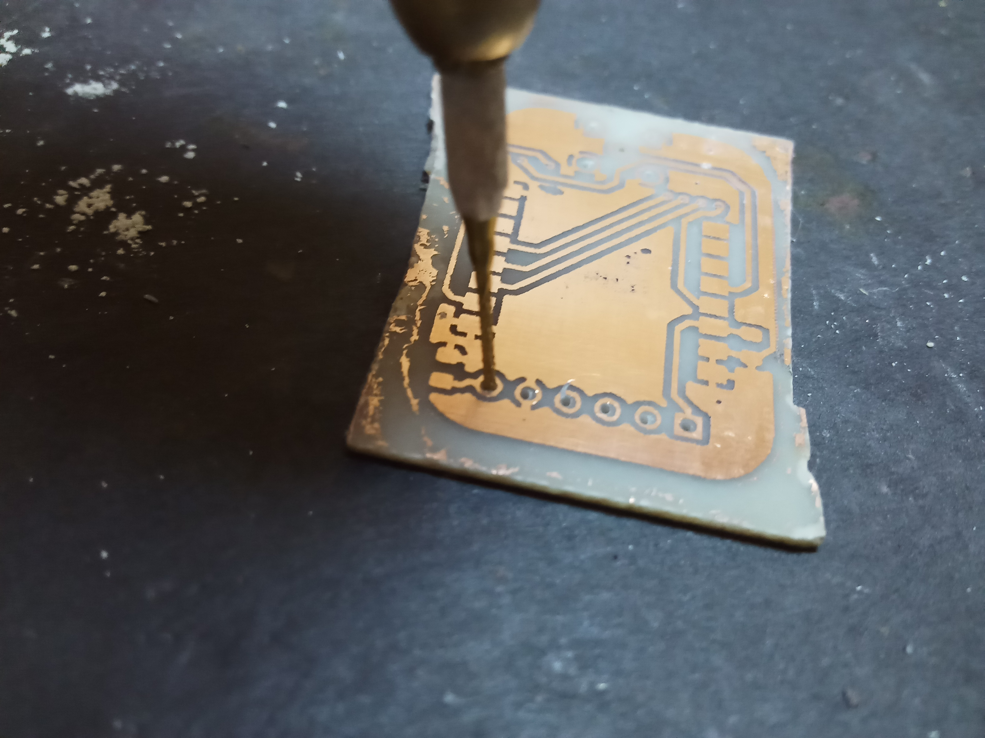
Drilling vias and through holes
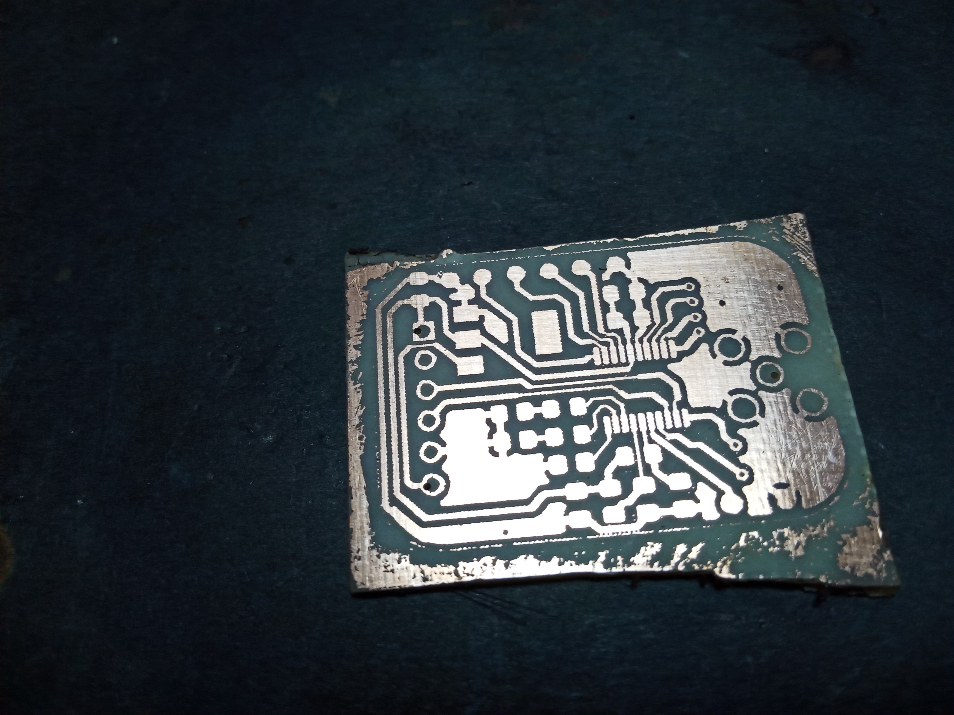
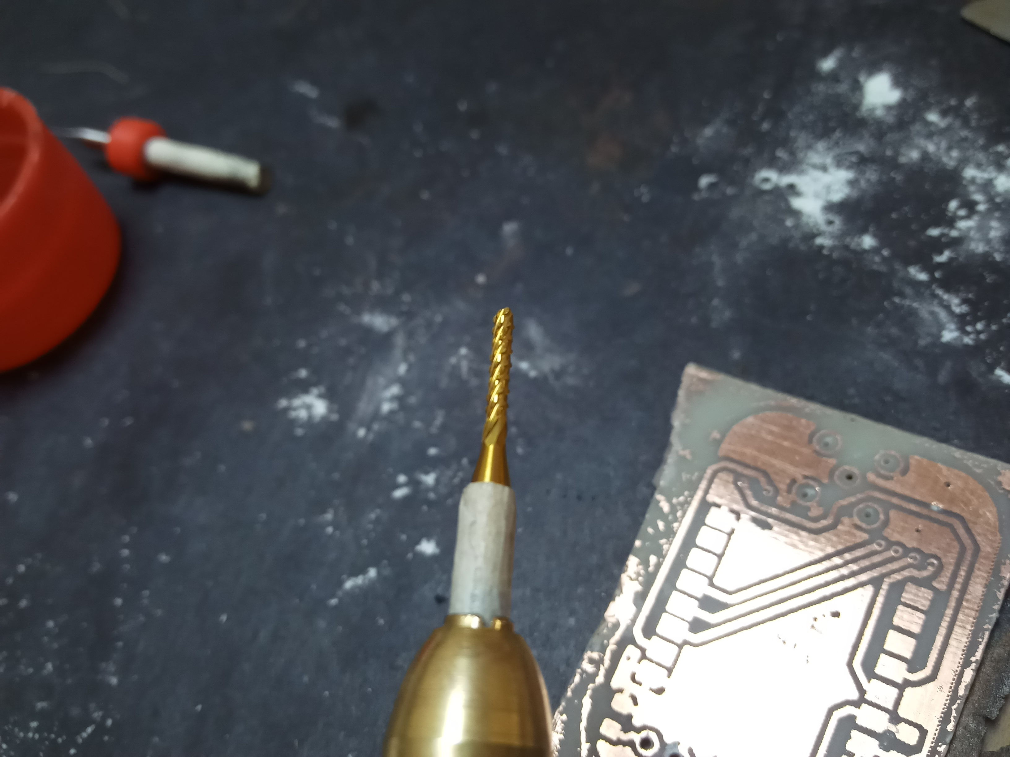
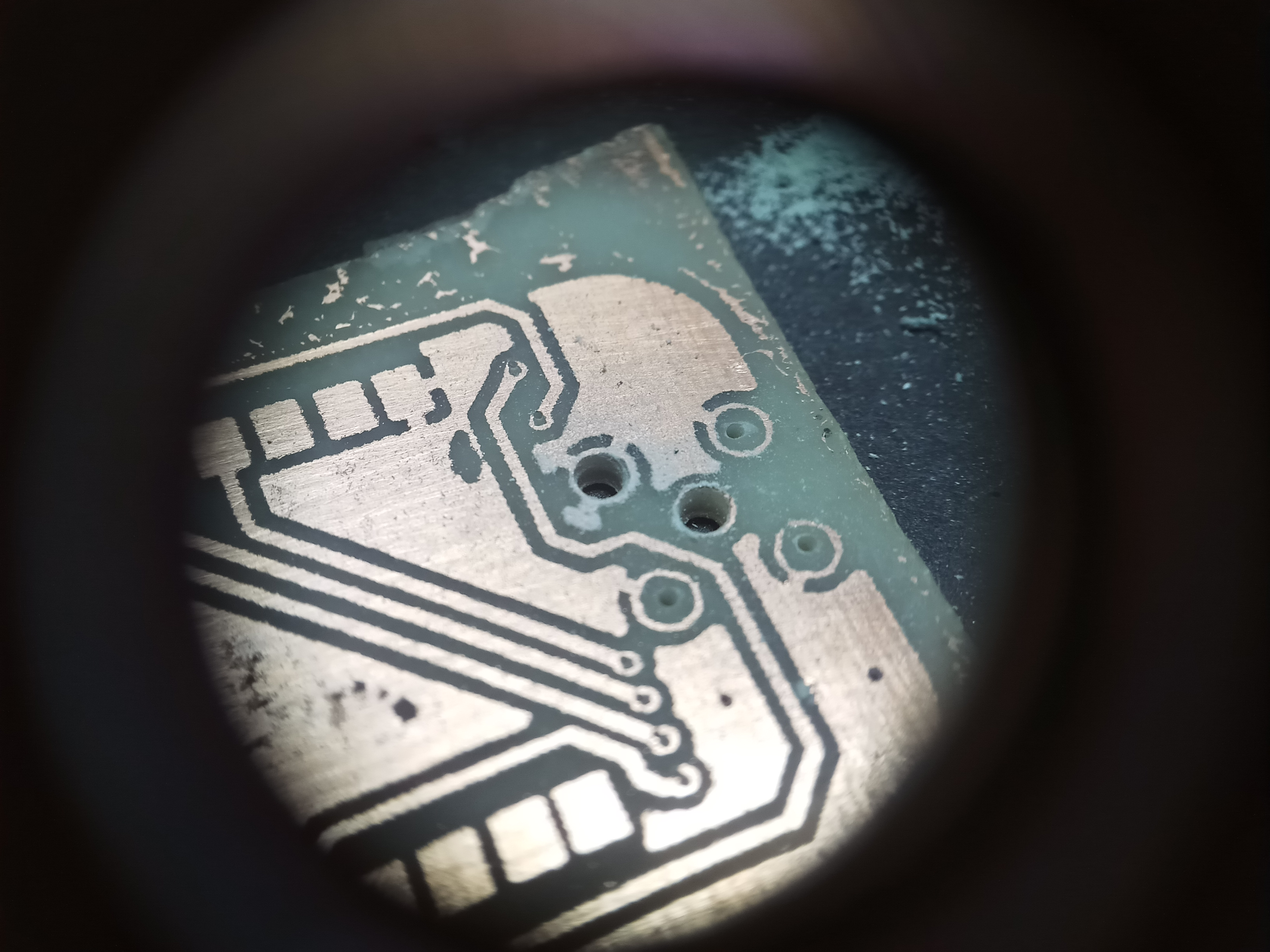
This is the moment of truth, to find out if all the effort we invested in aligning the layers has paid off. I like to start by drilling all the holes first with the smallest bit I have (0.3mm), then expanding them later as necessary. Do not worry if the holes end up slightly off centre.
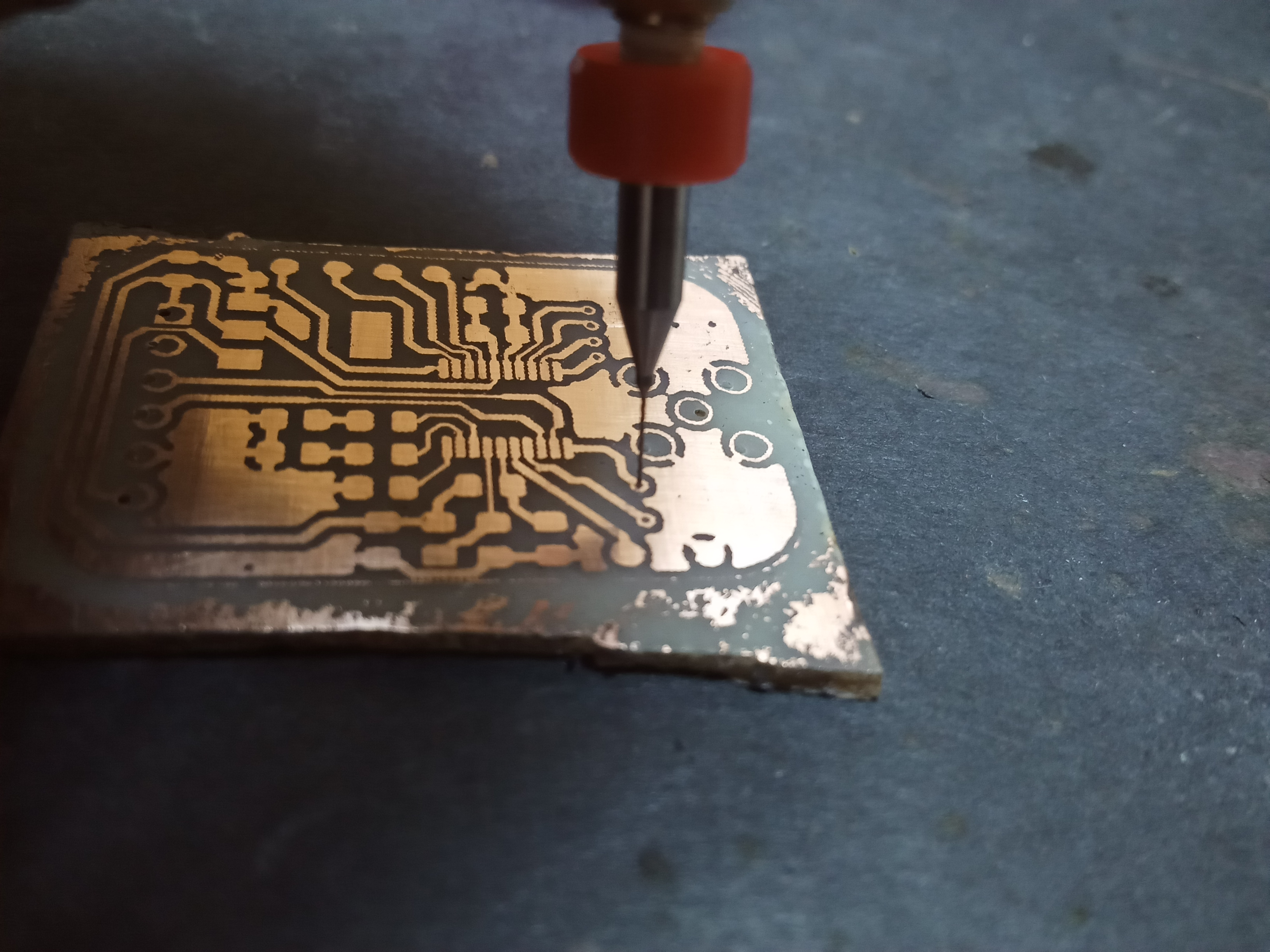
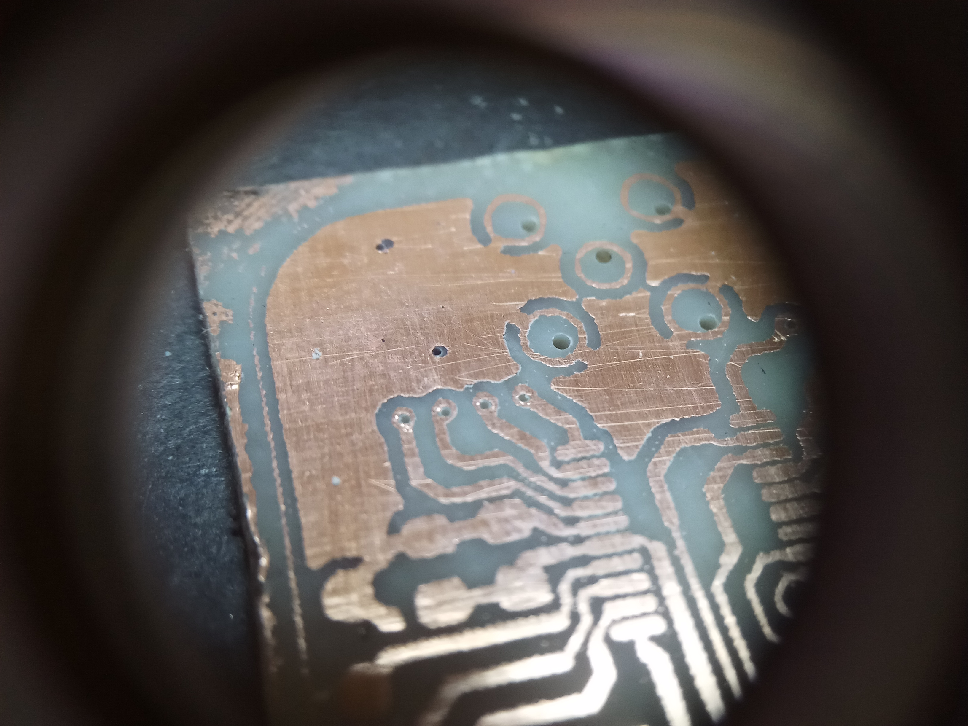
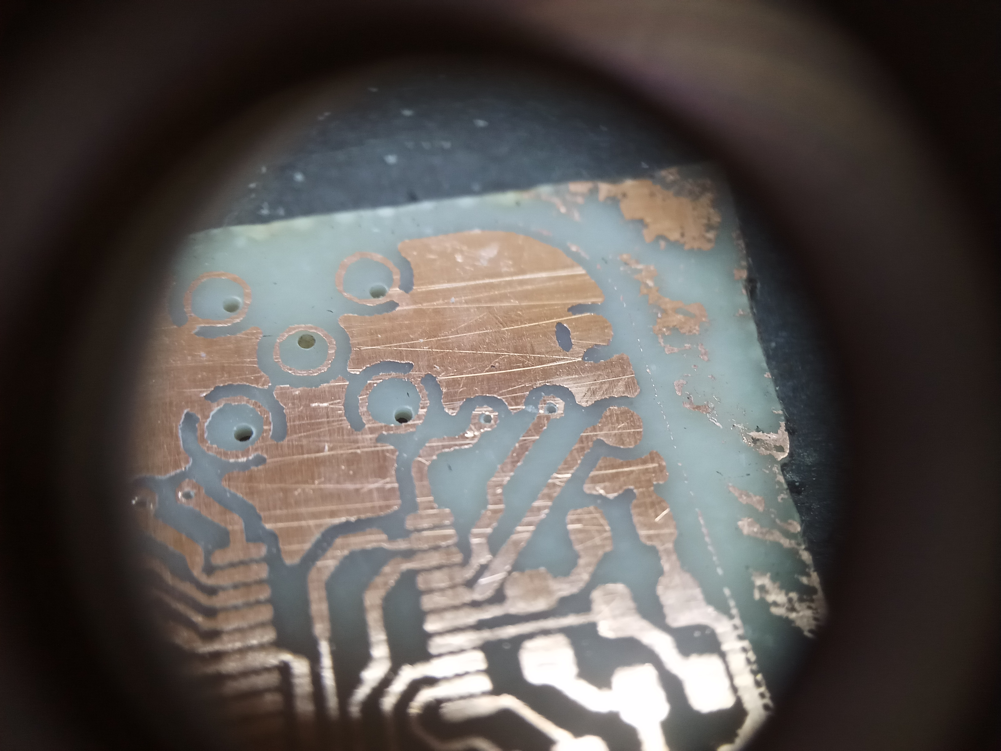
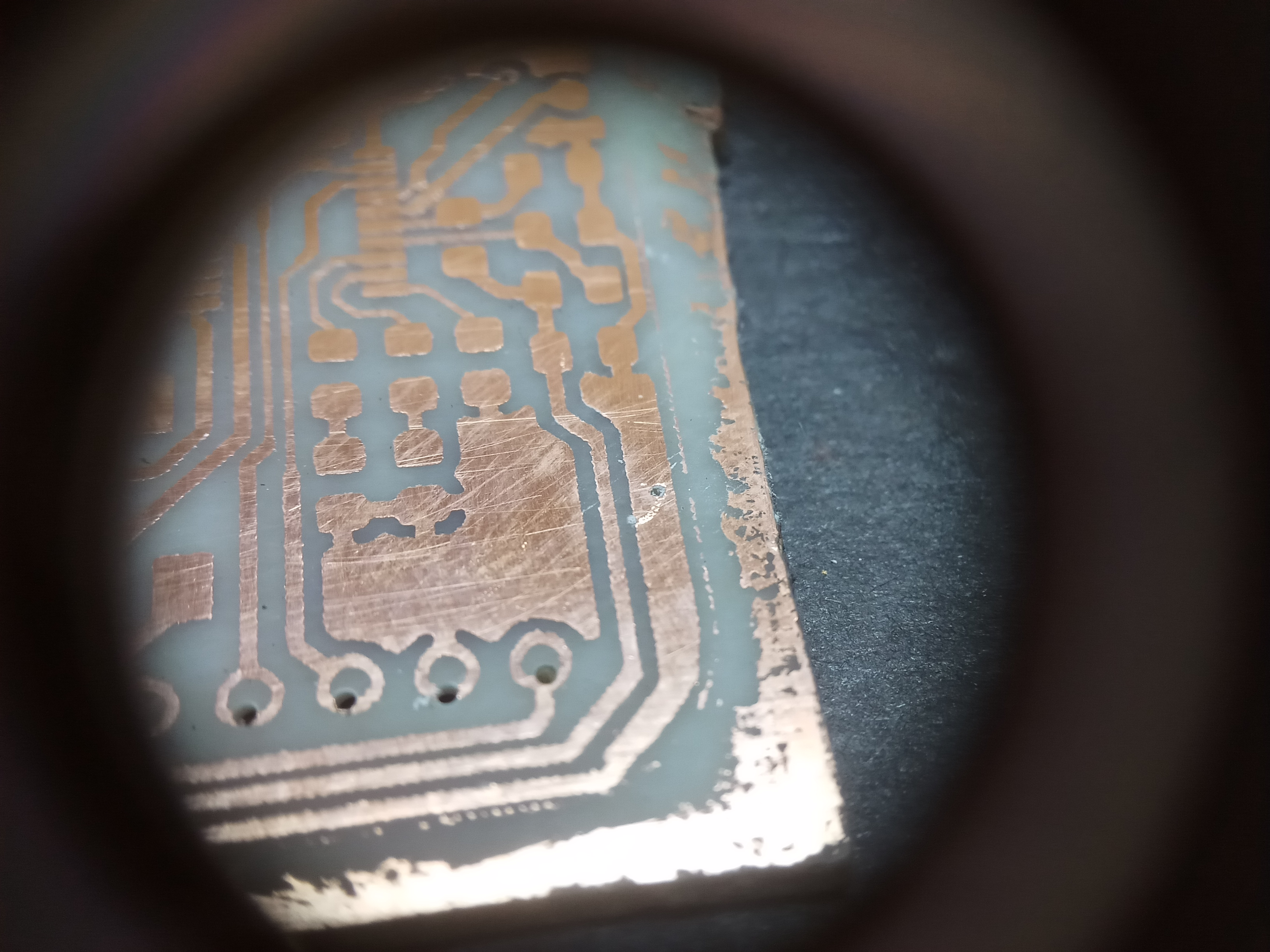
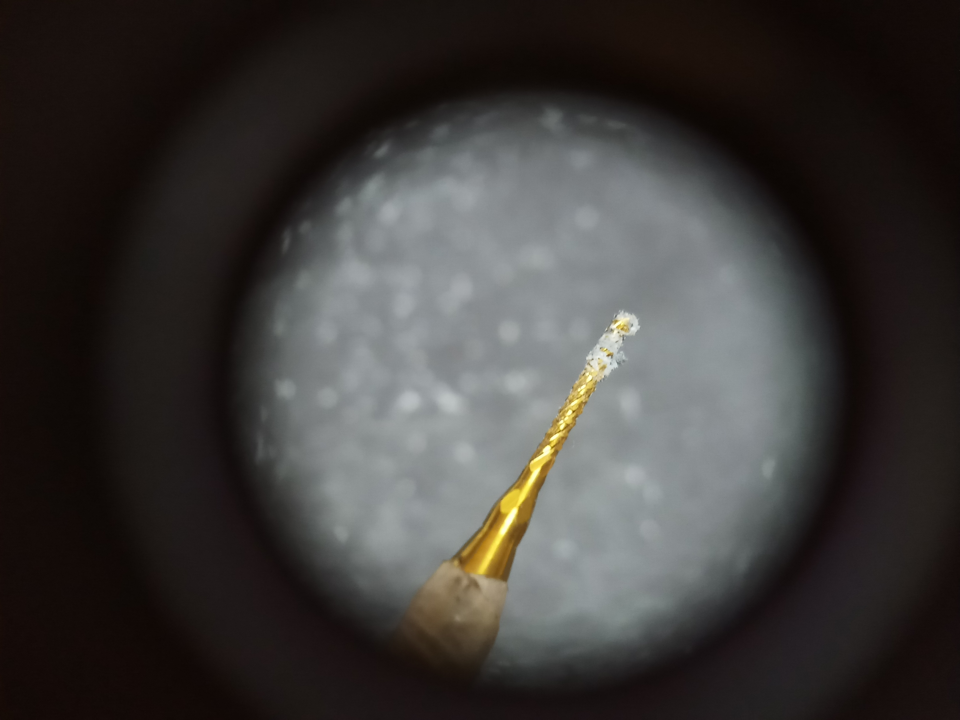
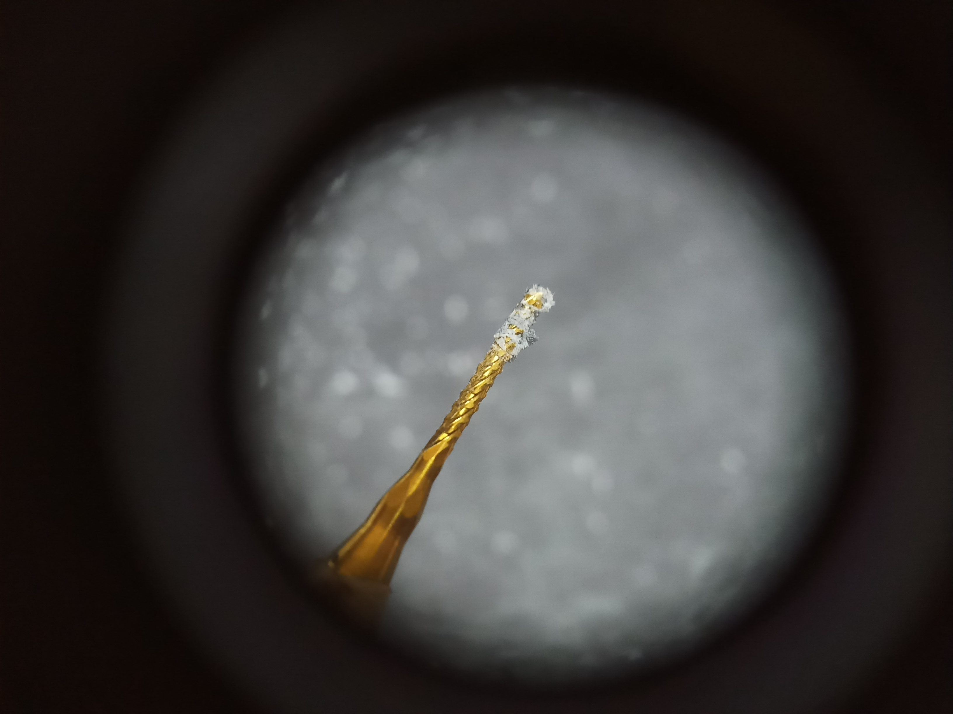
Next, expand the through holes using the appropriately sized engraving bits. I am using a 0.8mm engraving bit to expand all the regular through holes and 2mm for the SMA connector which has a bigger pin size. If your 0.3mm pilot hole was off centre, try to correct it at this point.
Tip:
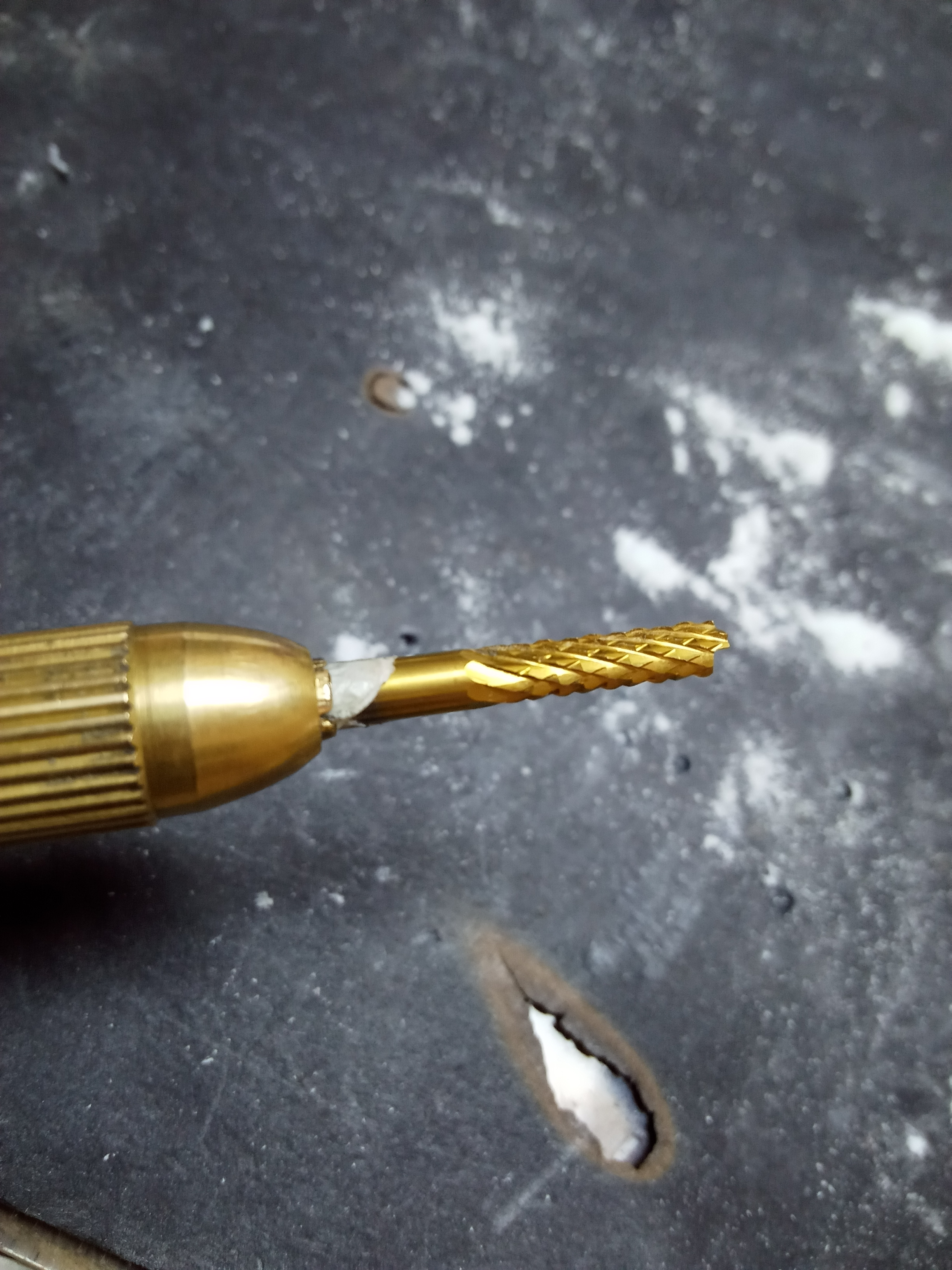
- The milling bits have teeth around their outer surface that easily snag a lot of material during the drill process expecially if your drill surface is made of plastic/acrylic like mine. There is probably a better way to clean it off, but I just run a sharp edge across the length of the bit while the drill is running until the bit is clean.
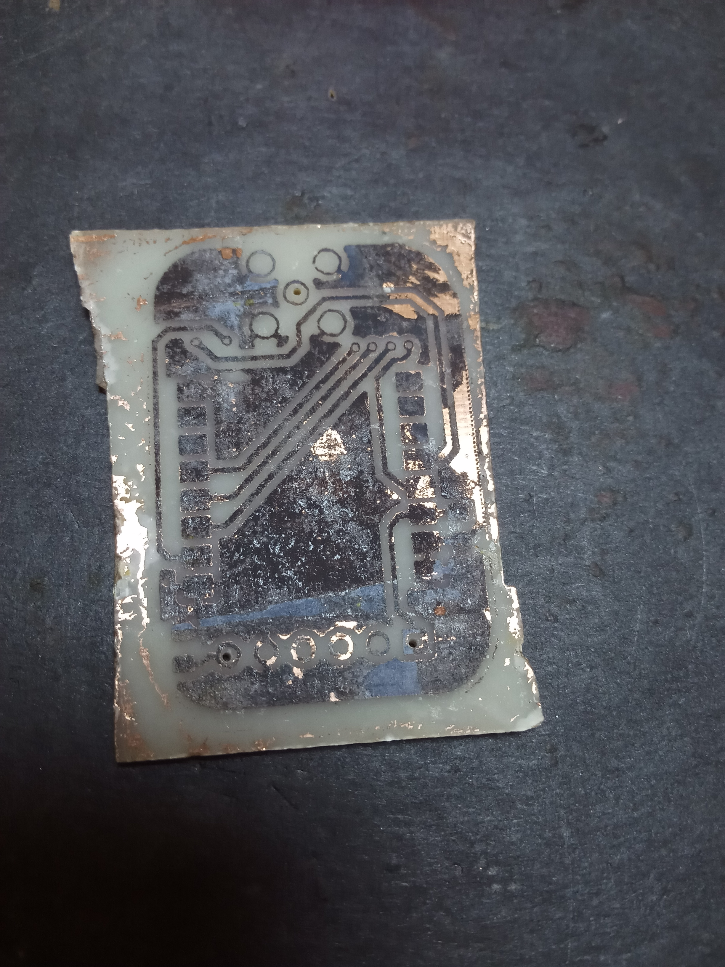
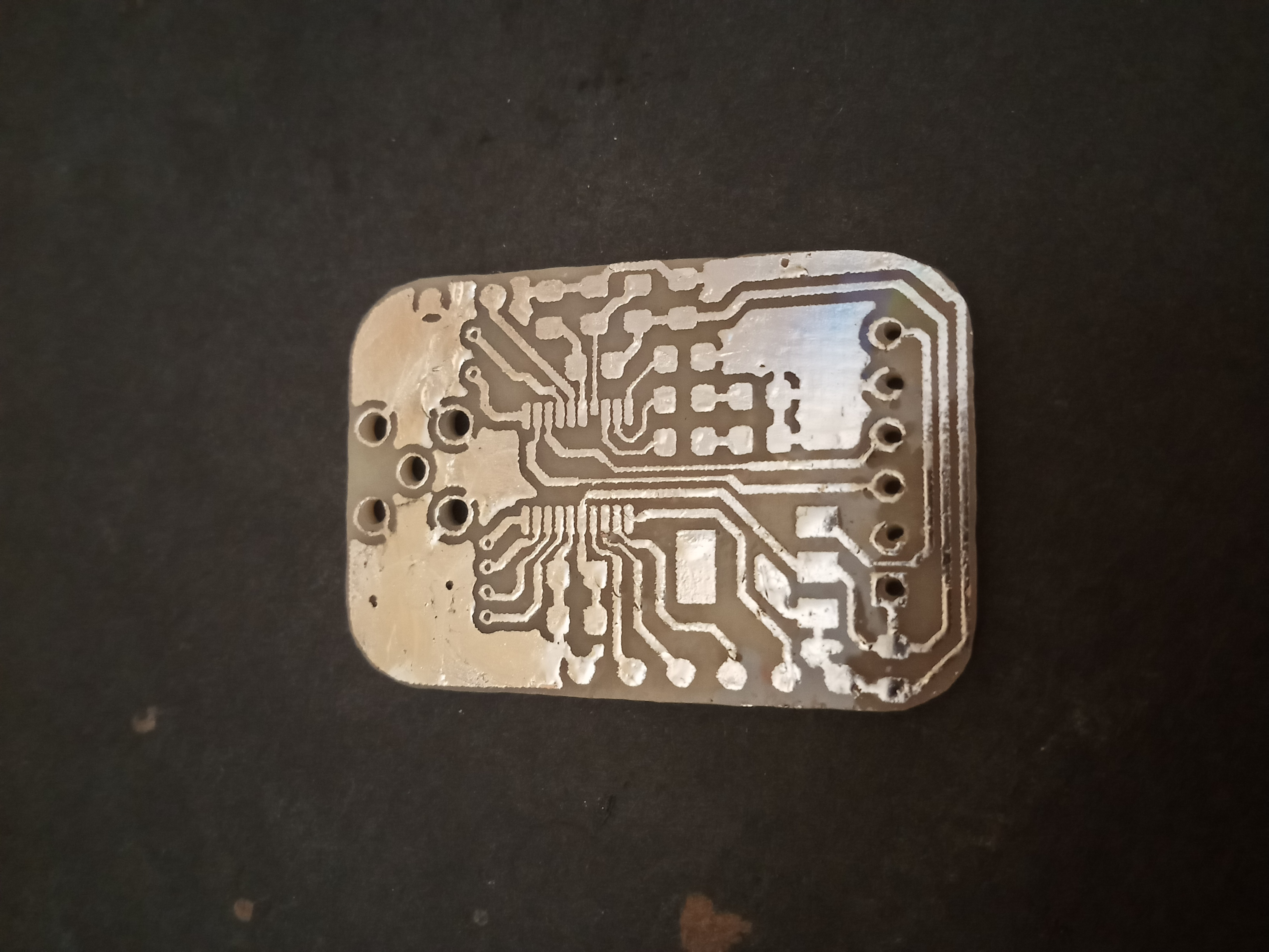
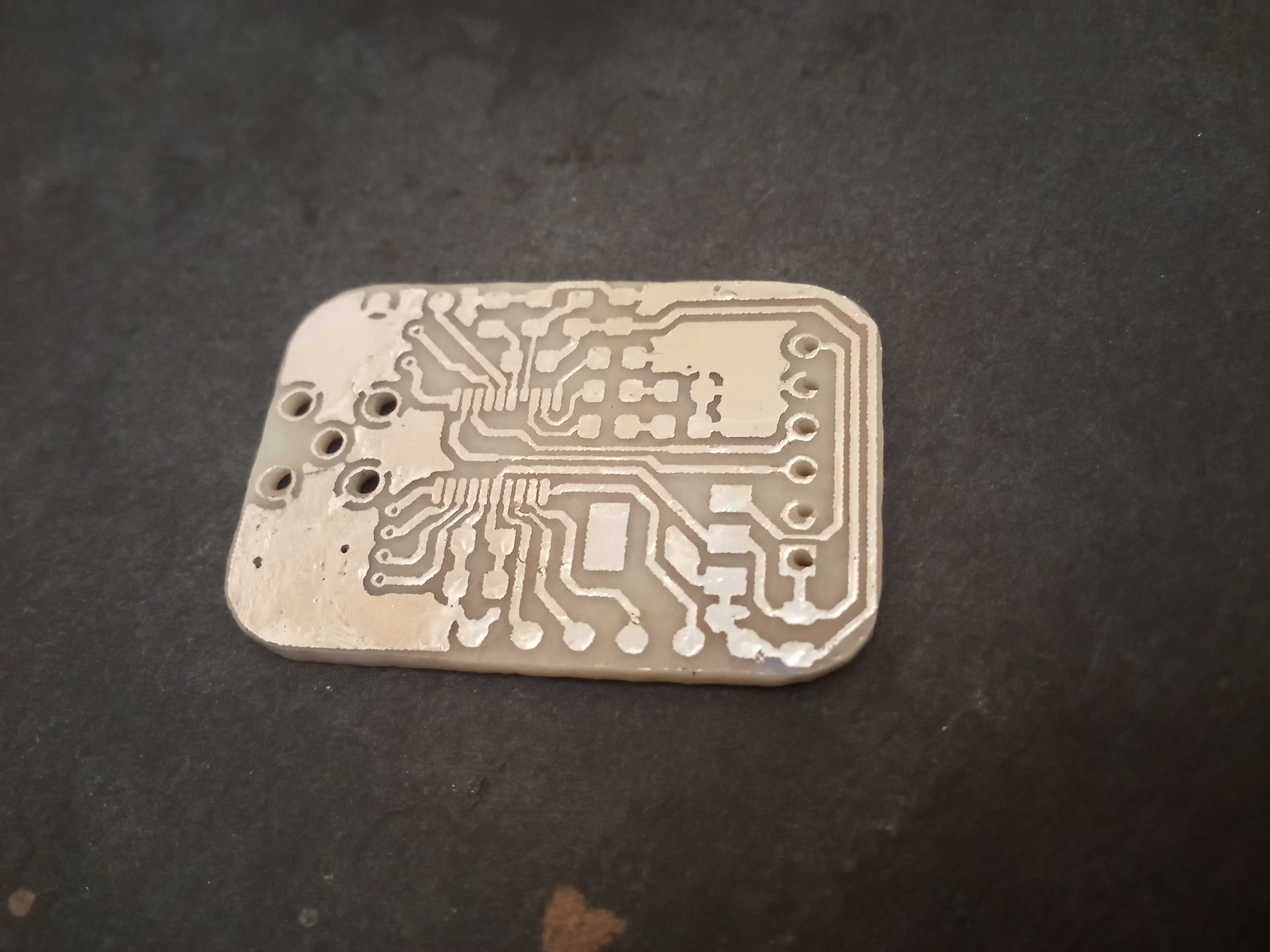
Tinning
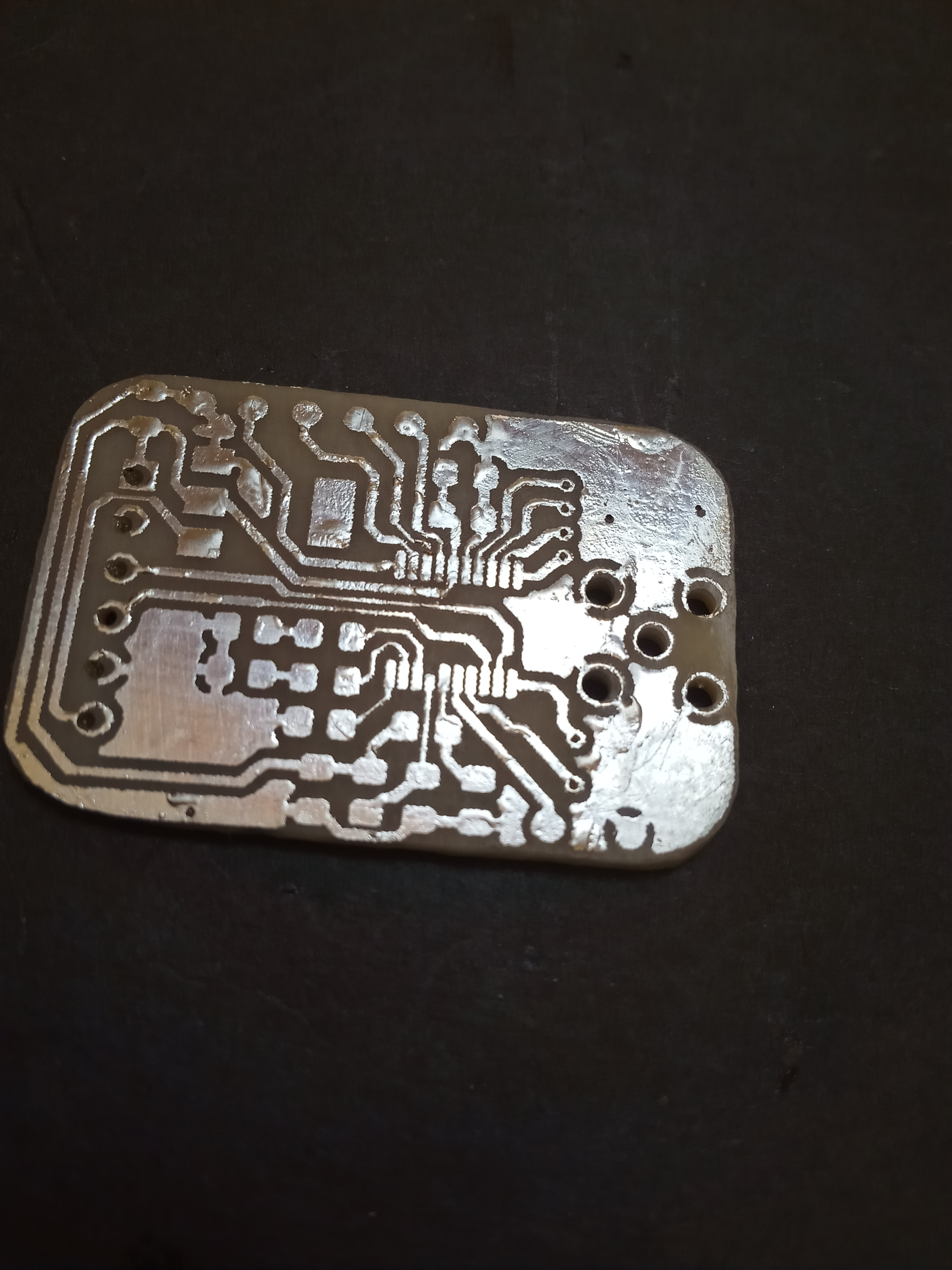
If you have reached this point, give yourself a pat on the back. You have done a great job! The PCB is now functionally complete. But, as you may remember from Part 1 of our homemade PCB series, a standard 2-layer board has soldermask as well as silkscreen layers that respectively protect the copper and mark out component designators. We may explore the use of these layers to give your homemade PCBs a professional finish, but for now, we make do with what we have readily available: solder.
By adding a thin layer of solder over the entire copper surface of our PCB, we protect it from oxidation, and - very conveniently - prepare the surface so that no extra solder is required during the soldering process.
Safery Warning:
- Make sure to carry out this step in a well-ventilated area as fumes from solder are known to cause respiratory disorder with long exposure.
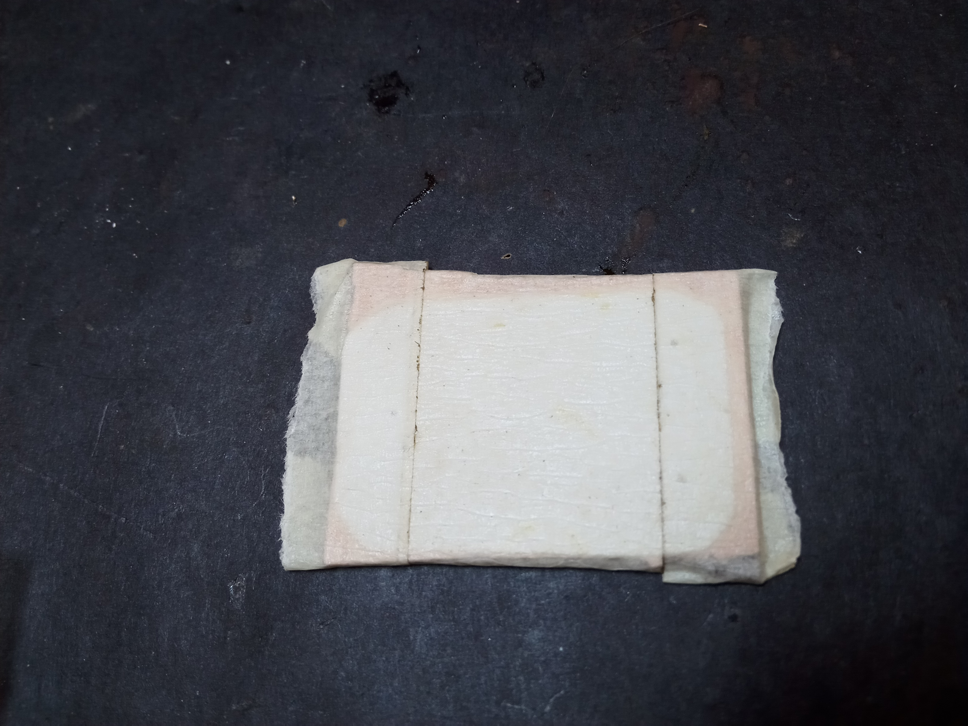
Start by wetting a short length of solder wick which we will use as our applicator to achieve even distribution of solder. Next, apply flux on the PCB so that the entire surface is covered. Things get a little fiddly here as you might need helping hands to hold your PCB in place; using a hot soldering iron as a paint brush and the wetted length of solder wick as its bristles, we 'paint' over the PCB surface, with the aim of getting as even a consistency as possible. You might need to add more flux in case what you have is not enough.
'Plating' vias and through holes
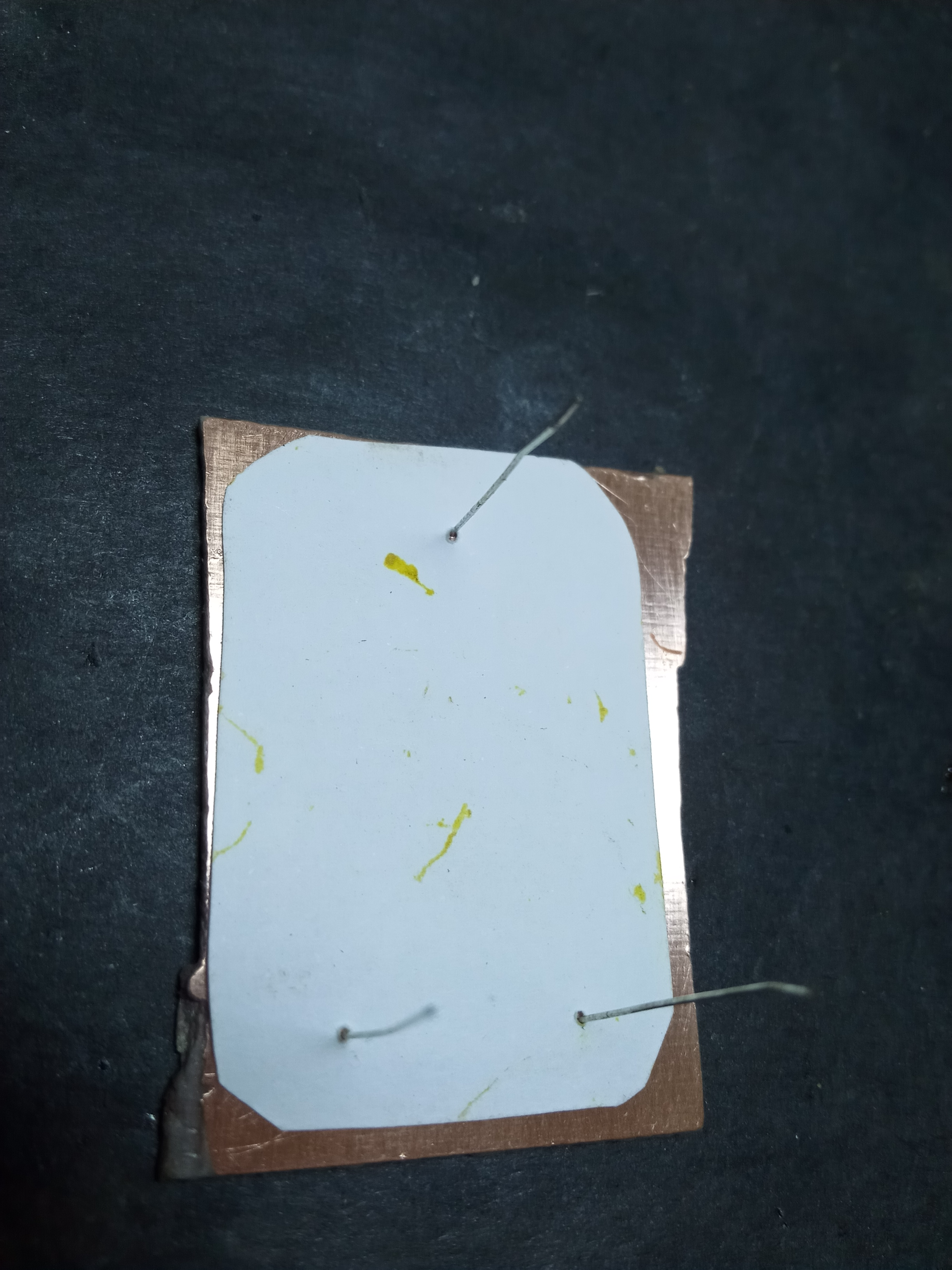
A via is a plated hole connects the tracks on one layer of the board to the tracks on another layer, allowing signals to be passed between components on the top and bottom layer. We have already drilled all the via holes in the right dimension; all that is left is to place conductive material through the via that will form an elctrical path.
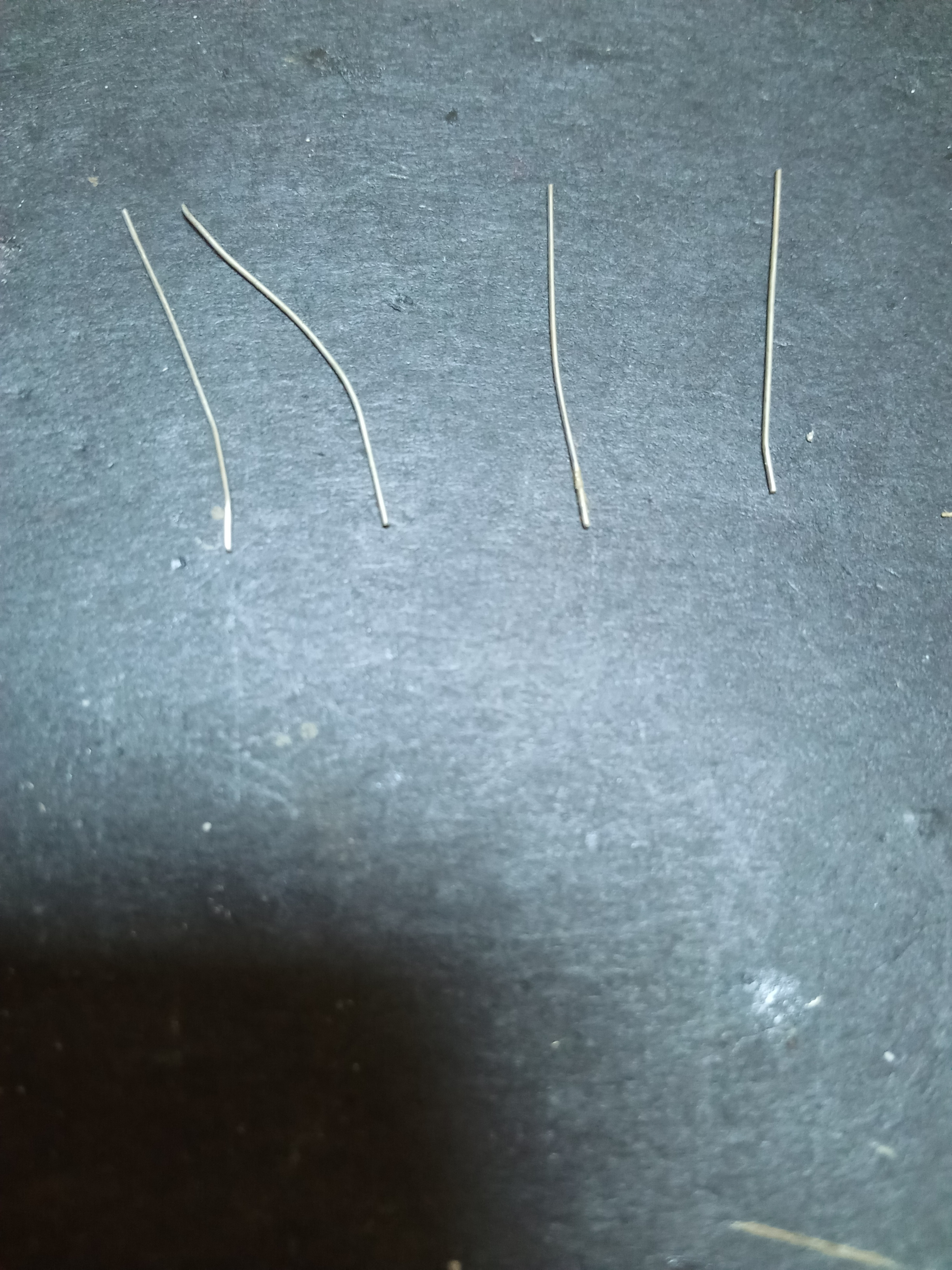
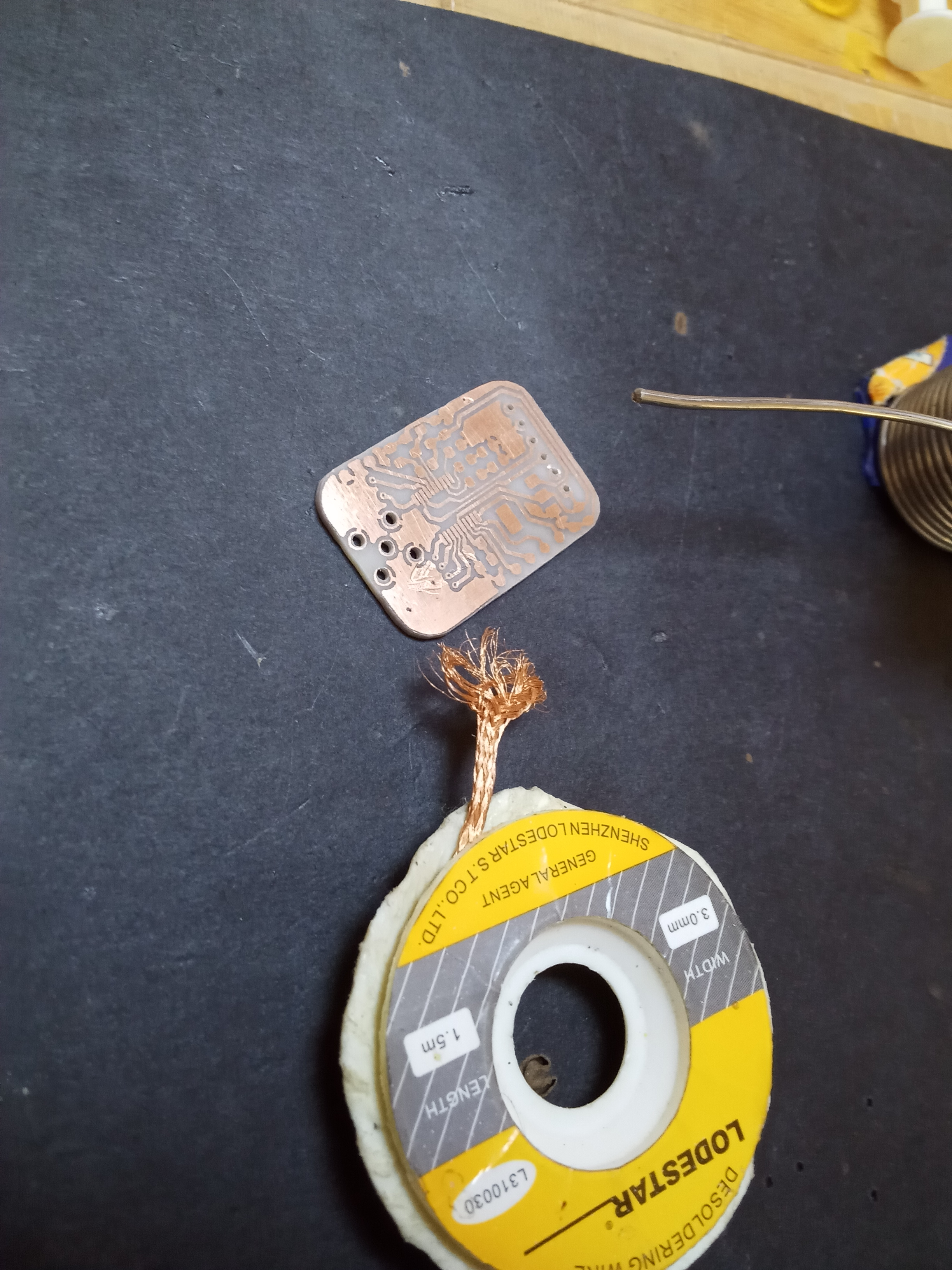
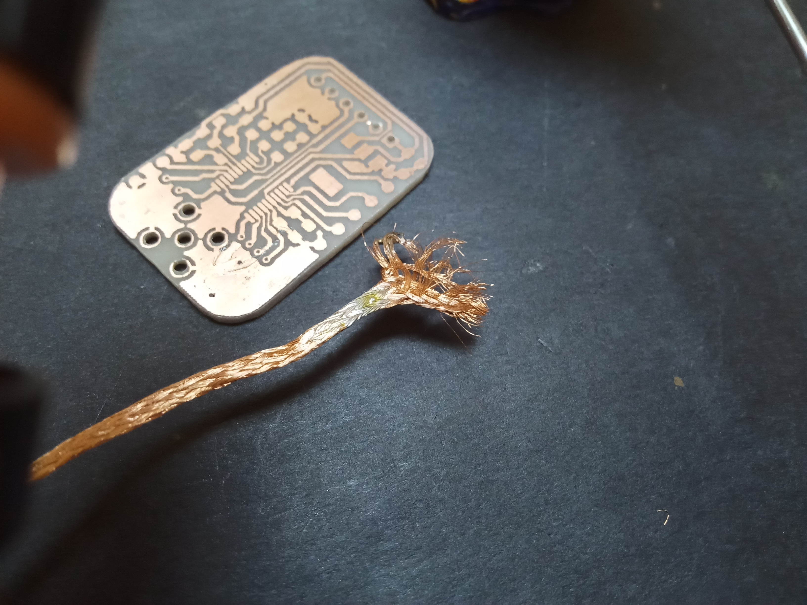
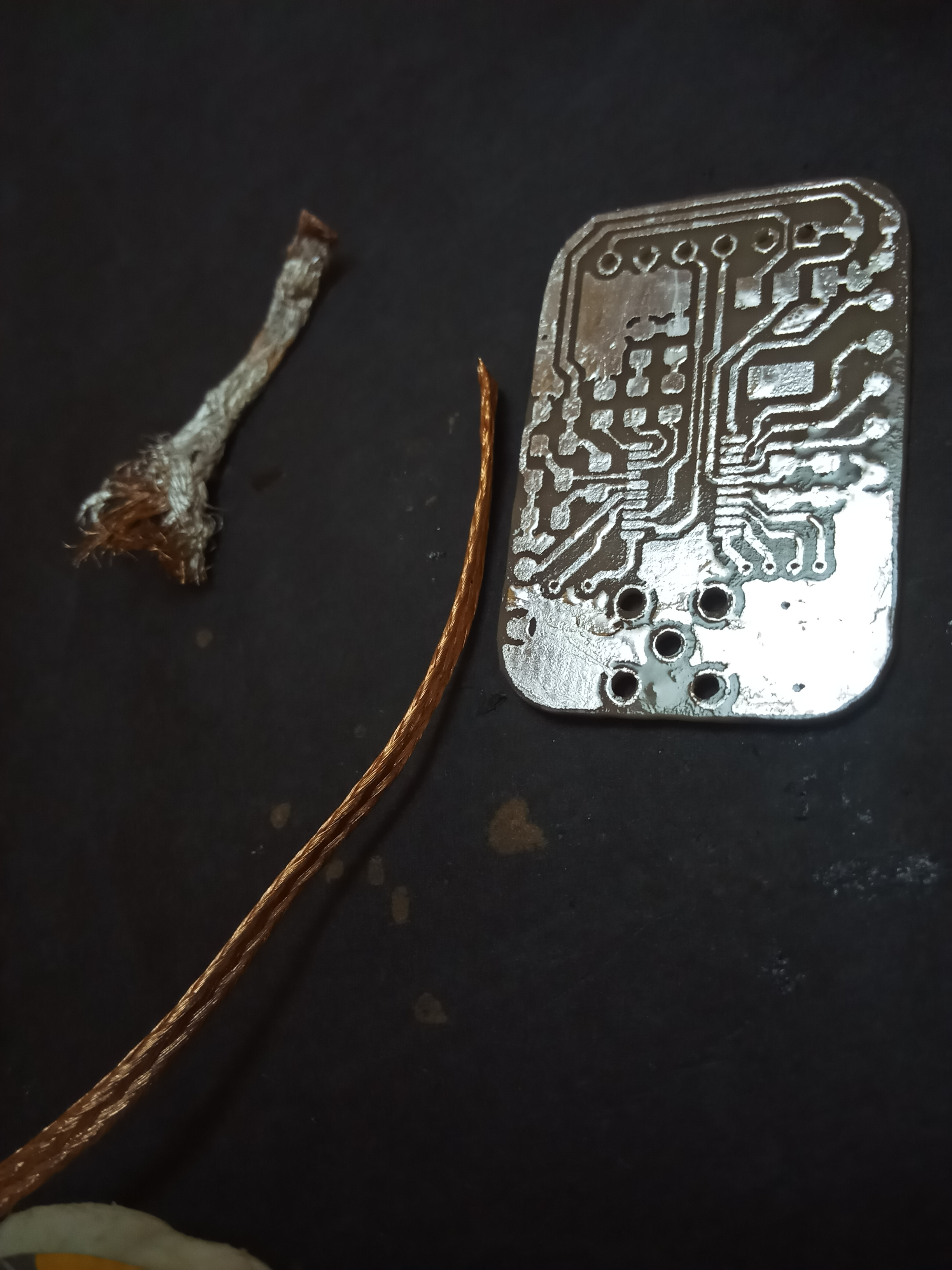
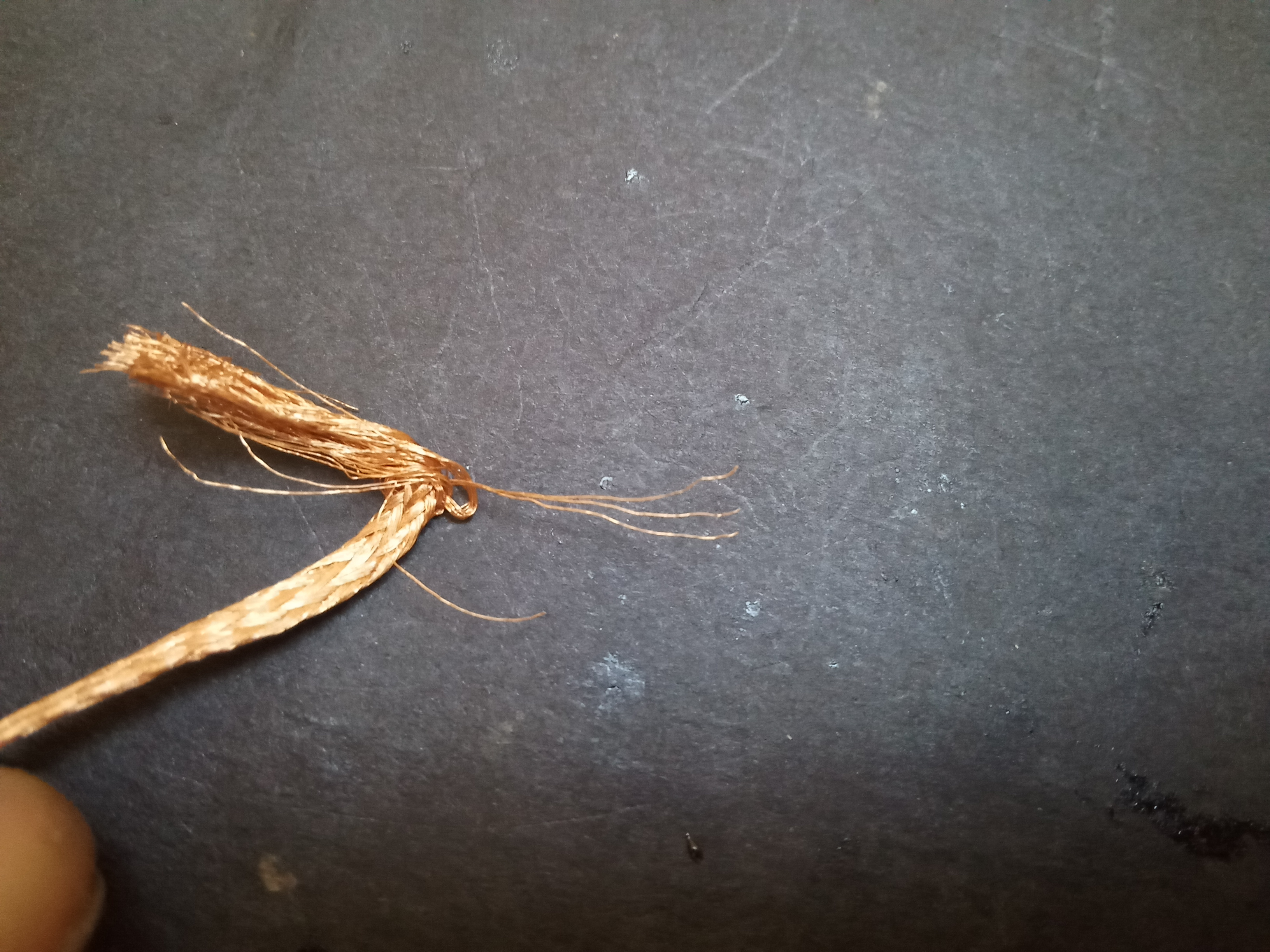
We start by picking a few strands of solder wick, twisting them into a braid, then wetting them with solder to bind them into a single conductor. The best way to wet wire with solder is to bring the wire in contact with solder then bring the hot soldering iron in contact with the two so that wire is between the solder and the iron.
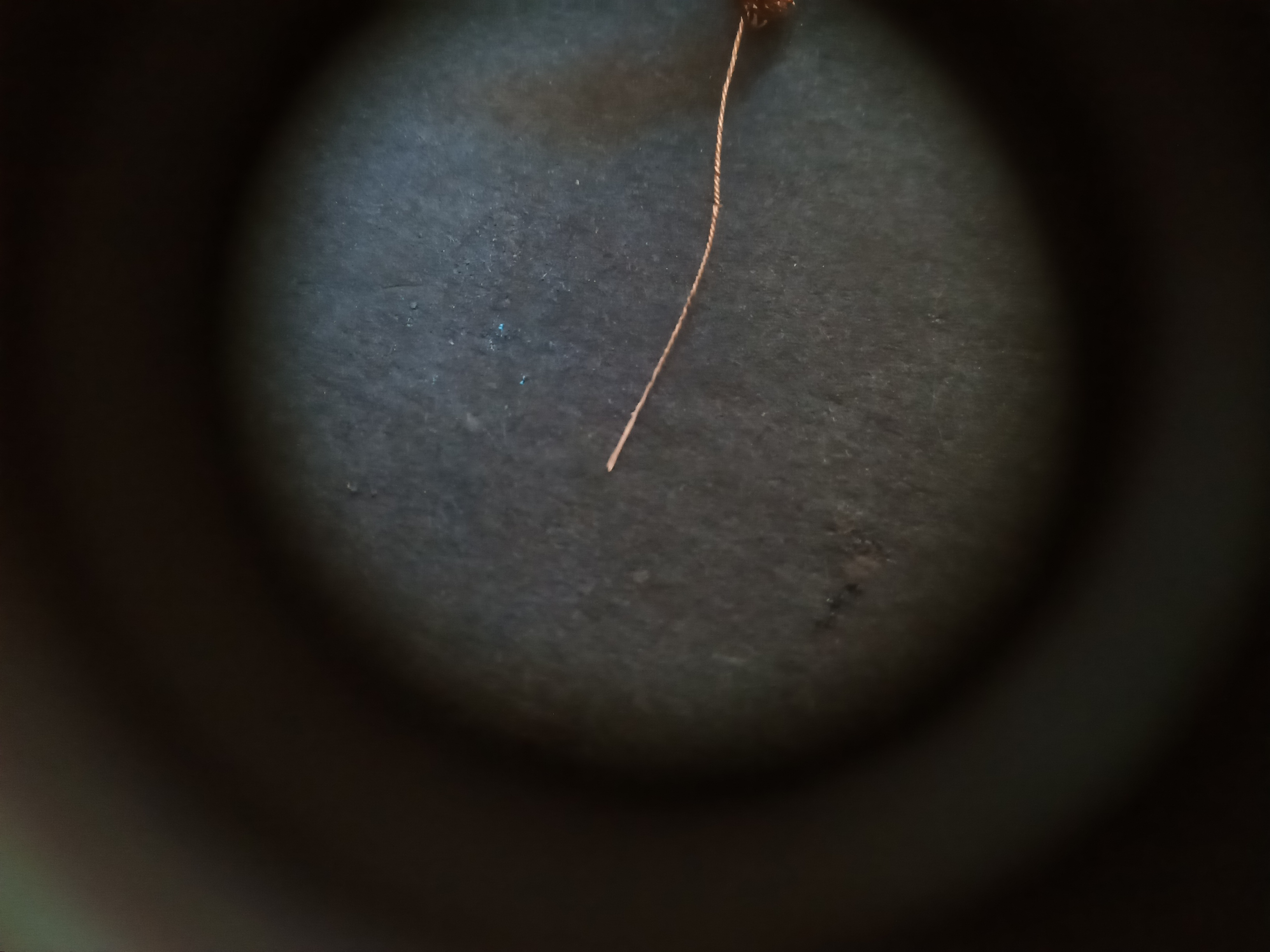
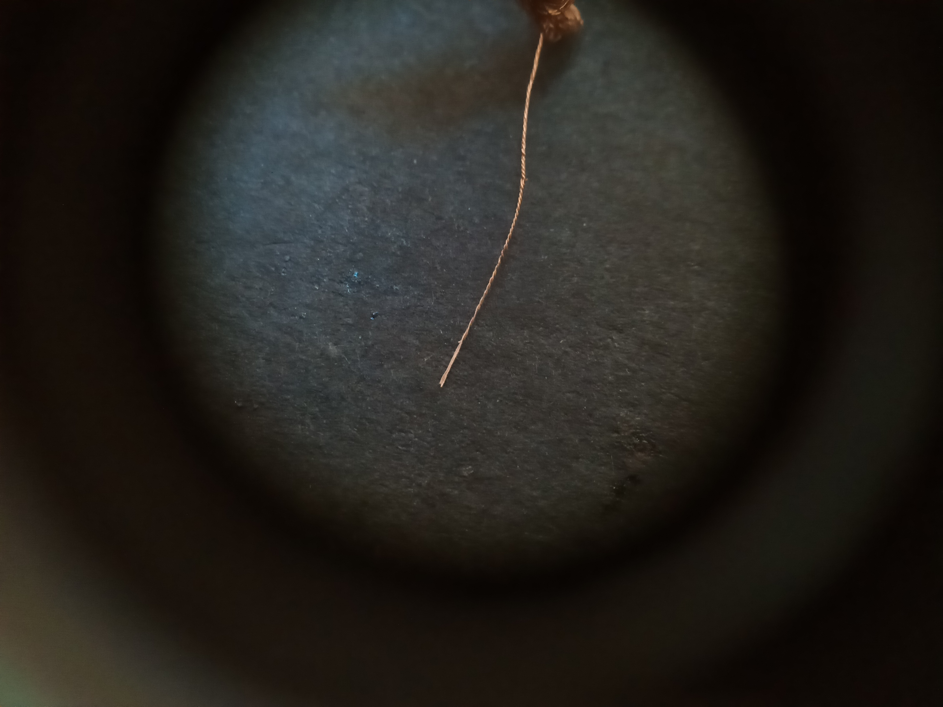
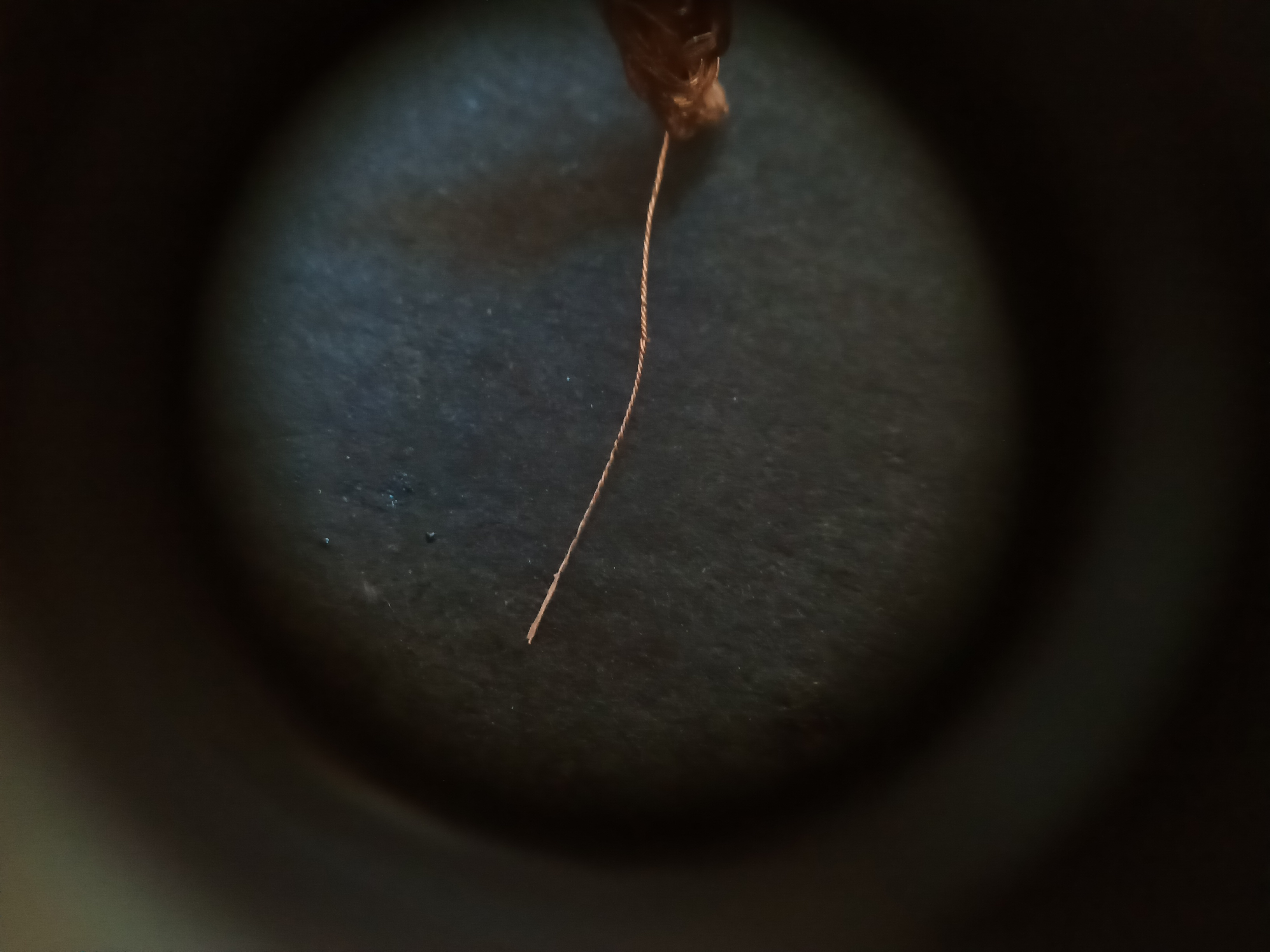
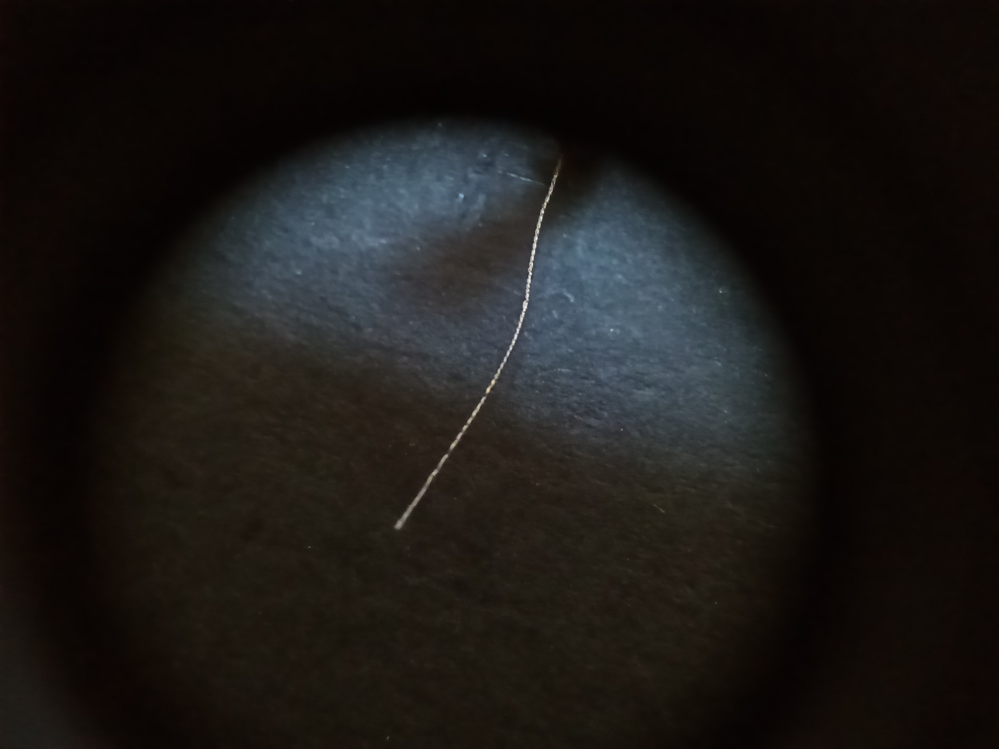
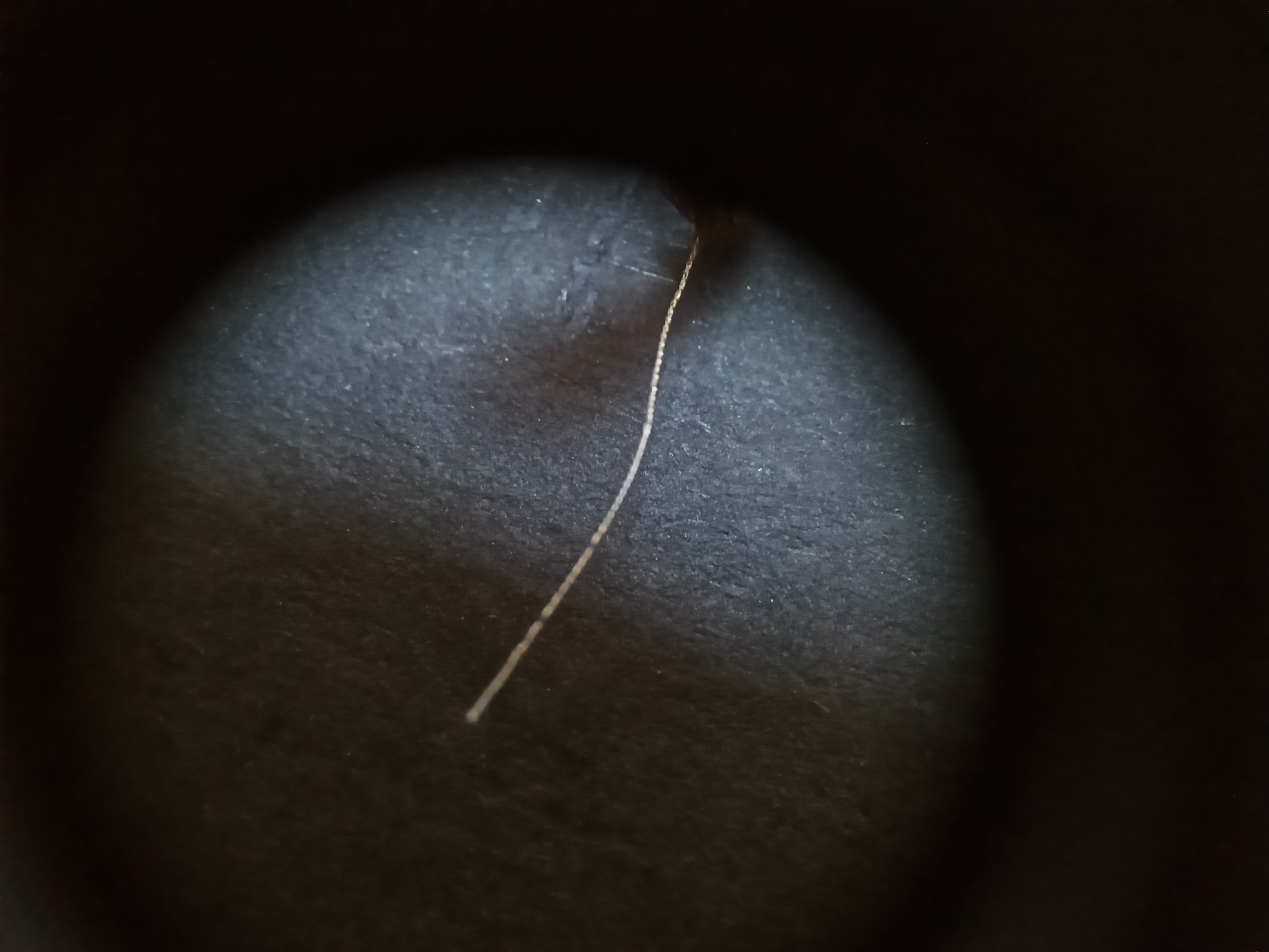
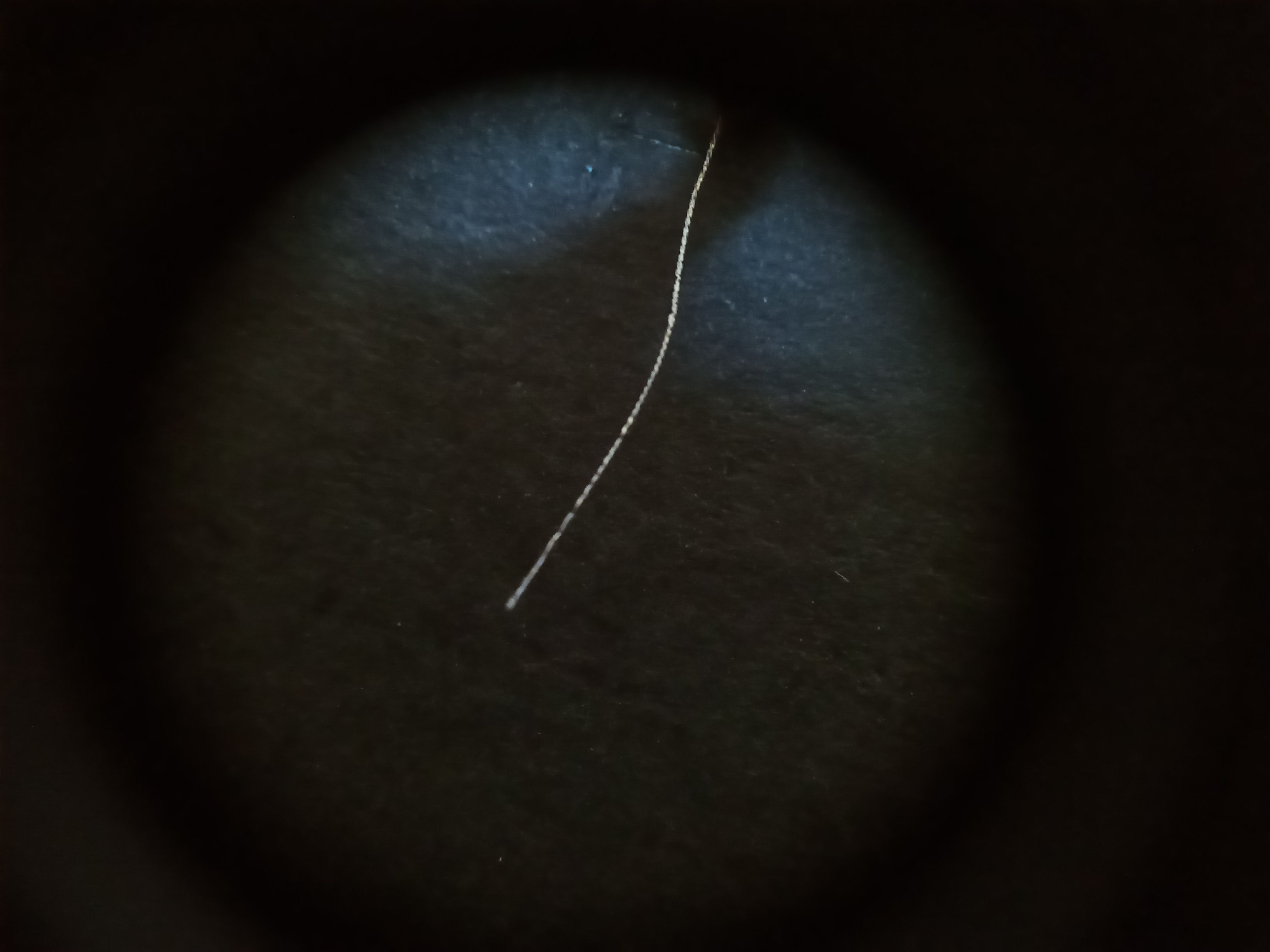
Next we snip off a short length of the tinned wire, thread it through the via and lay the overhang down on both sides so that it is on top of the tracks it is supposed to connect. Then to make the connection permanent, touch the part of the wire in contact with the track with your hot soldering iron and the solder within the wire should spread onto the track, bonding the two. Remember to do the heating on both ends of the via wire. Repeat this process for all other vias and through holes in much the same fashion, and the board is done!!
…and now for your hard earned dose of dopamine ;-)
Comments